Working with PCB Footprints
Create professional footprints that match your team's requirements and design specifications.
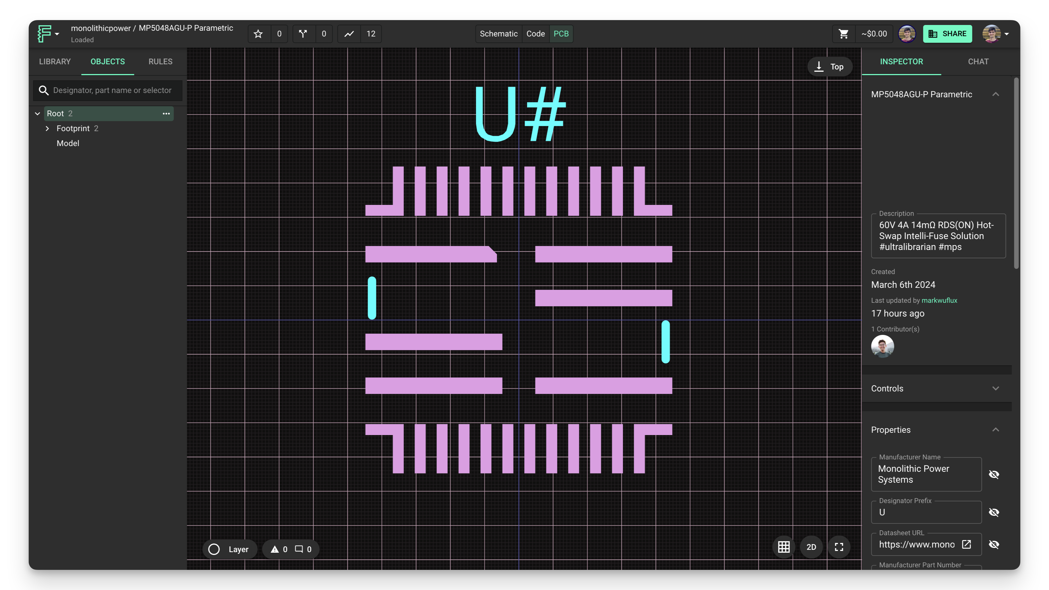
Overview
In this tutorial, we'll cover how to work with the PCB Editor to create custom footprints for your components. Whether you're designing a footprint from scratch or modifying an imported footprint, these techniques will help you create accurate, manufacturable component layouts.
Footprints define the physical layout of components on your PCB, including pad sizes, shapes, positions, and silkscreen markings. Creating precise footprints is essential for successful PCB manufacturing and assembly.
Adding Pads
The first step in creating a footprint is adding pads for component pins or leads. Pads are the copper areas where component pins make electrical contact with the PCB.
Every terminal you add in your schematic will have a corresponding pad in the PCB Editor. If you want to add a pad that doesn't need to be connected to other pads (a mounting hole for example) follow the steps below:
Click on the "Footprint" node in the right-side panel under "Objects"
- If you don't have a "Footprint" object, click on the three dots of the "Root" object and add a Footprint.
Click on the three-dots menu of the "Footprint" object and "Add" a "Pad."
Note: If you want to connect this pad to a terminal in the future, match the designators on the terminal and pad together.
To add pads to your footprint:
- In the PCB Editor, click on the "Objects" tab in the right panel
- Right-click on the footprint and hover over "Add"
- Select "Pad" from the menu
- Click to place the pad on the canvas
- Repeat for each pad needed in your footprint
Setting Pad Position
Precise pad positioning is crucial for component alignment and manufacturability. You can:
Method 1: Drag and Drop
- Simply click and drag pads to position them visually
Method 2: Precise Positioning
For exact placement:
- Select the pad to move
- Navigate to the "Object Specific Rules" in the right panel
- Find the
Positionrule - Enter the desired x and y coordinates in millimeters
- You can also use "in" and "mil" for inches and mils (thousandths of an inch)

Modifying Pad Size and Shape
After positioning your pads, you'll need to set their size and shape according to your component's specifications.
Individual Pad Modification
To modify a single pad:
- Select the pad
- In the right panel, add the "Pad Size" and "Pad Shape" rules
- Set the desired dimensions and shape
- Optionally, add "Pad Type" to create a through-hole pad
Batch Pad Modification
To modify multiple pads at once:
- Use selectors to target specific pads
- For all pads, use the "pad" selector
- For specific pads, use #Designator (e.g., "#VCC, #GND, #A0")
- Apply the same rules to all selected pads
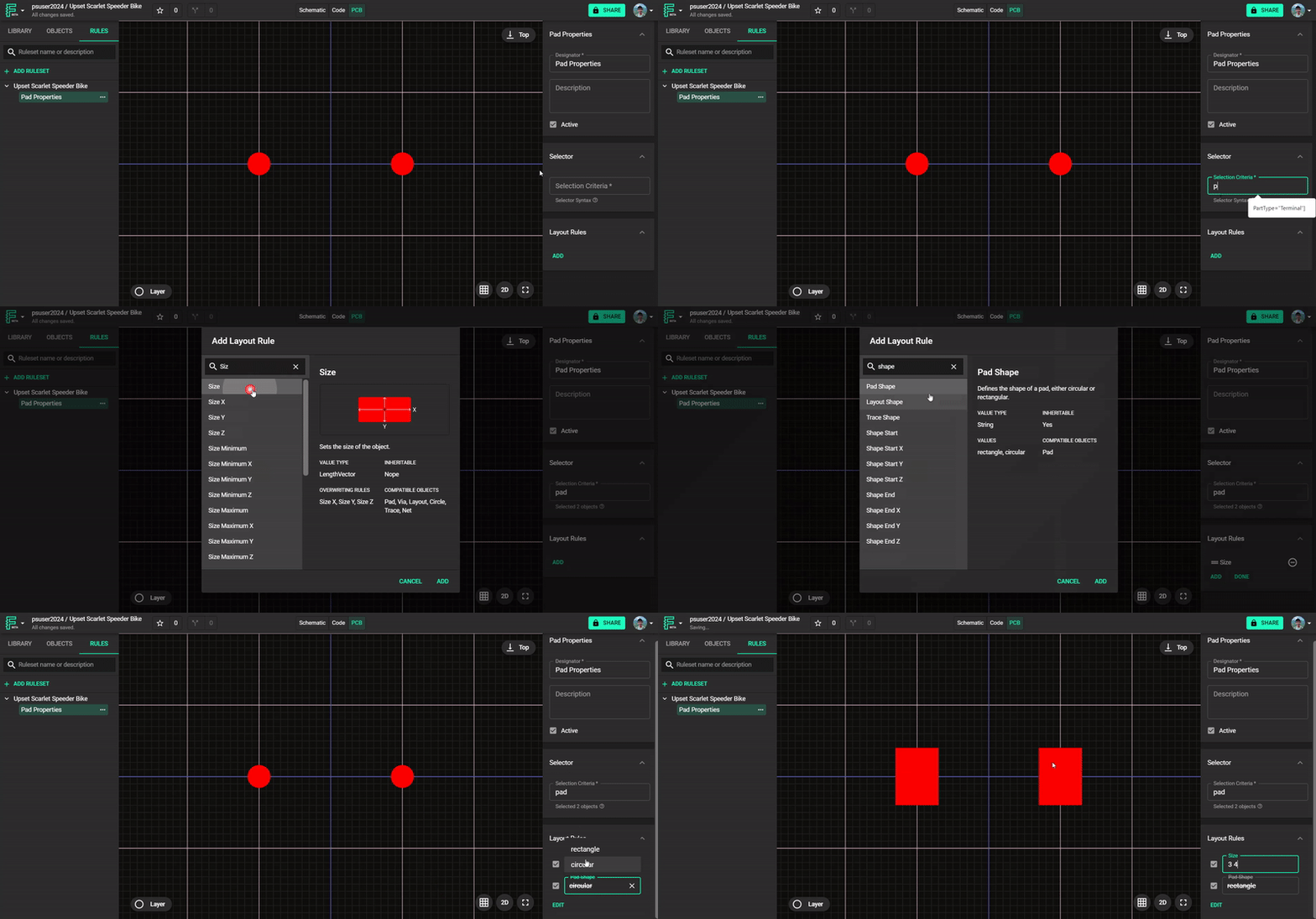
For advanced pad shapes and customizations, refer to our Custom Pad Shapes tutorial.
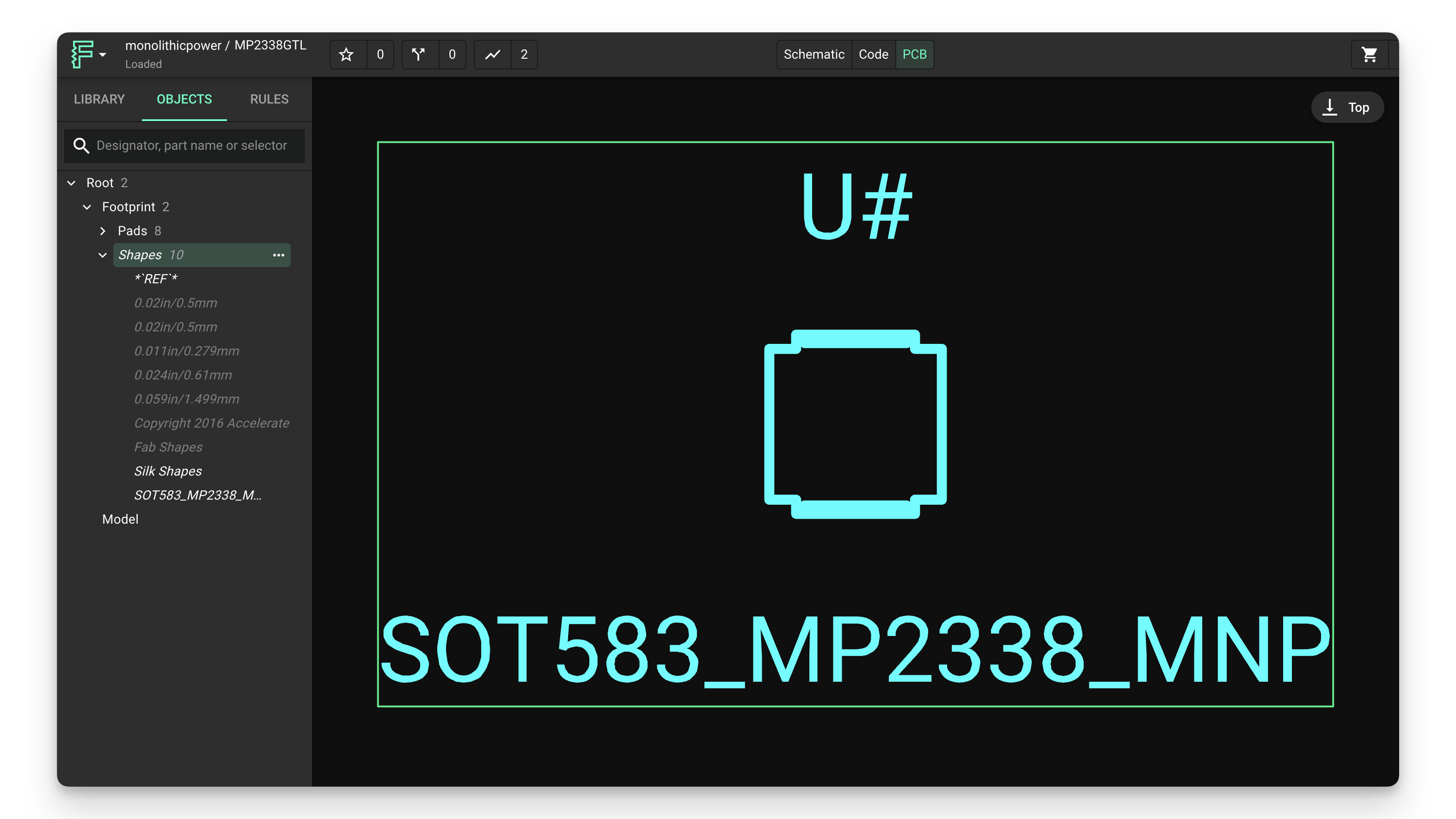
Adding Silkscreen Shapes
Silkscreen markings help identify component orientation and boundaries during assembly. To add silkscreen elements:
Adding Silkscreen Lines
- Click on the "Objects" tab in the left panel
- Right-click on the footprint, hover over "Add", and select "Silk line"
- Add the
Shape StartandShape Endrules to the silk line - Enter the desired x and y position values for each endpoint
- You can also drag endpoints or rotate lines (Right-click → Rotate)
- Repeat to create an outline of your component
Adding Text Labels
- Click on the "Objects" tab in the left panel
- Right-click on the footprint, hover over "Add", and select "Text"
- Add the
Contentrule to the text node - Enter the desired text (e.g., component reference, pin 1 indicator)
- Position the text appropriately
Setting the Origin
The origin point defines the reference position for your footprint when placed in a project. It's represented by the intersection of two blue lines in the PCB editor.
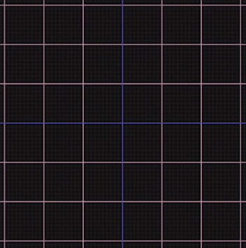
The origin placement affects how your component behaves when placed in a larger project:
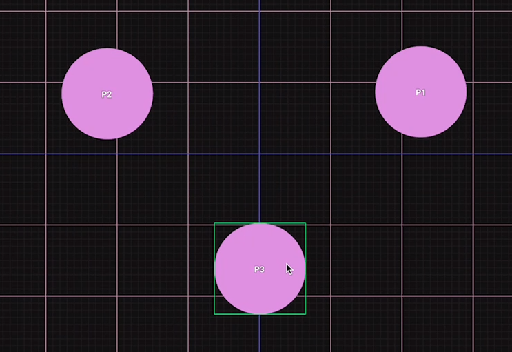
Centered Origin
For a centered origin (e.g., in a 3-pin part):
- Position pads symmetrically around the origin
- This makes the component's
locationrule correspond to the center of the component
Pin-Centered Origin
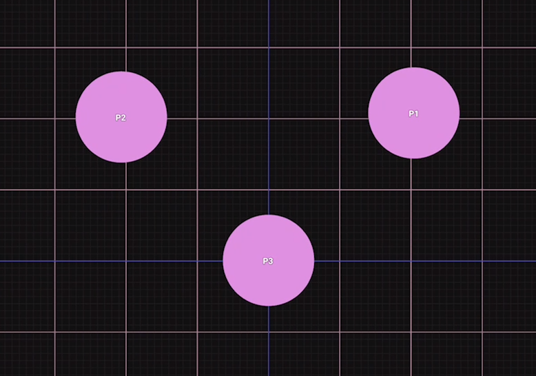
To center the origin on a specific pin:
- Position that pad at the origin (0,0)
- This makes the component's position correspond to that specific pin
Best Practices for Footprint Creation
- Follow datasheets precisely: Always refer to manufacturer datasheets for exact dimensions
- Include adequate clearance: Design footprints with appropriate clearance for manufacturing tolerances
- Add polarity indicators: Use silkscreen markings to clearly indicate pin 1 or component orientation
- Consider thermal relief: For high-power components, ensure adequate thermal management
- Standardize when possible: Use industry-standard footprints when available for consistency
Troubleshooting Common Issues
Pad Alignment Problems
- Double-check all measurements against the datasheet
- Ensure you're using the correct units (mm, mil, inches)
- Verify that the origin is set appropriately for your component
Silkscreen Issues
- Make sure silkscreen lines don't overlap with pads
- Keep text size appropriate for manufacturing capabilities
- Ensure polarity indicators are clear and visible
Footprint Compatibility
- Test your footprint with the actual component if possible
- Verify pad sizes are appropriate for both soldering and the component leads
- Check that the footprint works with your manufacturing process constraints
What's Next
Now that you've learned how to create footprints, you might want to explore:
- Working with Symbols - Learn how to create schematic symbols for your components
- Custom Pad Shapes - Discover how to create specialized pad geometries
- Publishing to the Library - Share your footprints with your team
- Creating a Complete Part - Combine footprints with symbols to create complete components