Flux supports multi-layer designs. In this tutorial, we'll cover:
- Configuring the board stack-up
- Moving objects between layers
- Routing across multiple layers
Configuring Board Stack-up
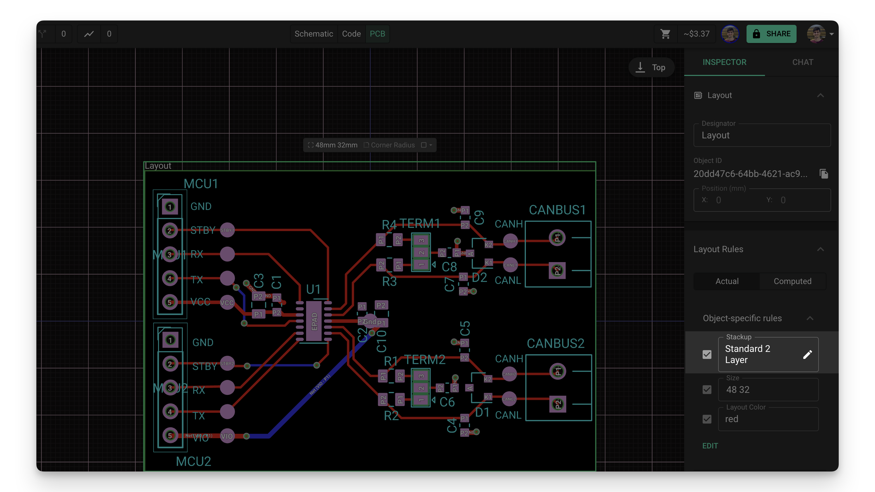
New projects are configured with a 4-layer stack-up by default. Here's how to configure a different stack-up:
- Go to the "Layout" object in the "Objects" tab on the right-side panel of the PCB editor
- Select the "Layout" object.
- In the right panel, add an "Object Specific rule" called "Stackup"
- Select a Stackup from the default list or click on the pencil icon to create a custom stackup with the Stackup Editor
When selecting a stack-up, consider your design requirements:
- 2-layer boards are suitable for simple designs
- 4-layer boards provide better signal integrity and power distribution
- 6+ layer boards are necessary for complex, high-density designs
Moving Objects Between Layers
There are two ways to move an object between different layers:
Using the "Layer" Rule
- Select the object you want to move to a different layer
- Find the "Layout Rules" menu on the right, and click on edit to add a new "Layer" rule
- Select the layer you want the object to be moved to from the list
The "Invert" Layer
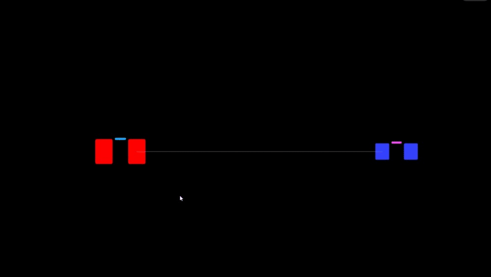
If you look closely, you'll find an extra layer on the list, called the "Invert layer". When this layer is selected, the object will be moved to the opposite layer in the stack-up. For example:
- An object in the Top layer will be moved to the Bottom layer
- An object in Mid-layer 1 will be moved to Mid-layer 2 in a 4-layer stack-up (or to Mid-layer 4 in a 6-layer one)
This behavior might look redundant for standard parts, but it allows more flexibility for modules. Imagine you have a module in your project that has components on the top and bottom layers:
- Assigning "Bottom" to the layer rule for this module will move every single one of its components to the bottom layer. This will likely result in several components on top of each other.
- Assigning "Invert" to the layer rule will flip every component to the opposite layer. Components in the top layer will end up in the bottom layer and vice versa. This will result in a fully-functional, flipped version of the module.
Using the "Flip Layer" Menu
There is a quick way to move an object to the opposite layer by simply right-clicking on the object and selecting the "Flip Layer" option. Keep in mind that this will assign the "Invert" layer to the object; please refer to the previous section for more information about the invert layer.
Routing Across Multiple Layers
To switch layers while routing a trace:
- Hover over the target component's pad until a green dot appears
- Click on the green dot to begin routing - the trace will follow your cursor on the currently selected layer
- To move the trace to a different layer, right-click and select the target layer
- A via will be automatically placed, connecting the two layers
- Continue routing on the new layer
Via Placement Best Practices
When routing across multiple layers, consider these best practices for via placement:
- Minimize via count: Each via adds impedance and manufacturing cost
- Maintain clearances: Ensure vias have proper clearance from other objects
- Consider thermal effects: Vias can help with thermal management by connecting to ground planes
- Via size: Use appropriate via sizes for your current requirements
- Via stitching: For ground planes, consider using via stitching for better connectivity