Using Layout Rules in Flux
Rules in Flux are all-encompassing and can dictate just about every aspect of your board, from trace widths to component clearances to silkscreen behavior.
Introduction
Flux's layout rules enhance the PCB layout process. While this tutorial covers the traditional approach of setting up layout rules through menus, we recommend using the toolbar for quicker and more intuitive property modifications when working with individual objects.
Gaining a strong understanding of Flux layout rules for printed circuit board design revolutionizes the layout process by actively applying rules during layout creation, preventing errors, and enhancing efficiency in real time.
Flux shines in that it utilizes design rules to layout the board and update in real-time as you design. Rather than checking a design against a set of design rules after layout completion, Flux uses the defined rules to create the layout entirely. Traditional EDA software, instead, checks for errors only after the design is completed, forcing users to go back and re-work designs.
In Flux, rules are something you actively use in the design process for PCBs. This workflow is special in that Flux design rules:
Apply in real-time
Can be applied to many components simultaneously
Apply changes to features in the PCB layout as soon as they are created
Don't need to be used for DRCs once a design is finished
Getting Started with Flux Layout Rules
In Flux, rules are not only design guardrails, but they can directly modify a design as well, essentially changing the properties of one or more objects. Some examples include:
A position rule applied to a capacitor component that dictates its location on the board
A trace-width rule applied to a net, that sets the width of all traces part of that net
A keep out rule that defines silkscreen clearance from all resistors

There are two main ways of applying a rule to the target object (trace, component, etc):
Selector-based rules, where a group of objects is selected based on a predefined condition, and the rule is applied to all of the selected objects. Learn more about selectors.
Object-specific rules, where a single object is selected manually for the rule to apply. Learn more about object-specific rules.
Object-Specific Rules
As the name suggests, object-specific PCB rules apply only to the selected object. Only Selector-based layout rules can be applied to multiple objects.
Adding an object-specific rule
To add an object-specific rule:
Select an object by clicking on it or using the "Objects" menu on the left
Find the "Layout rules" in the right-side menu
Click on "Edit" → "Add"
Search for the desired rule and add it

Examples
Let's create a rule for an individual net that requires an especially large current draw.
Method 1: Using the Toolbar (Recommended)
Select the desired net or trace in your PCB layout
The toolbar will appear automatically
Use the "Trace Width" option in the toolbar to set the desired width
Method 2: Using Object-Specific Rules
Select the desired net in the object tree
Navigate to the inspector toolbar on the right, and scroll down to the Object-Specific Rules under the Layout Rules section
Select edit and add a trace width rule, setting the value to an appropriate width necessary for safely passing the required current
All traces under the net in the object tree will then automatically update to the specified size.
It is also possible to add a ruleset with the selector set to [uid=_objectID_]to achieve the same result. You can find the object's ID by clicking on and copying it from the top of the inspector panel.
Selector-Based Layout Rules
As opposed to Object-specific layout rules, selector-based rules can apply to more than one object. To select which objects a rule will apply to, we use the concept of selectors (heavily inspired by the CSS Selector Syntax). If you're coming from other EDA tools, selectors are similar to queries. It's a syntax that allows you to select specific matching objects.
Adding a selector-based rule
Navigate to the PCB editor of your project
Select the "Rules" tab in the panel on the left of the screen
Choose the "New Ruleset" button, and a new item will appear underneath the project rules titled "New Ruleset"
Select "Edit" under the "Layout Rules" section of the right-hand panel and then click "Add"
Use the "Selection criteria" text box to type your selector
Add the rules that you wish to define in your currently selected ruleset
Select the value for each of the added rules
To help you understand what you're selecting, Flux will highlight objects that match your selector. Once you finish typing, bounding boxes will appear on the canvas and in the Objects list.
Selectors are case sensitive. For example, in the above screenshot, only trace will select all traces for you, but Trace will not select anything.
Examples
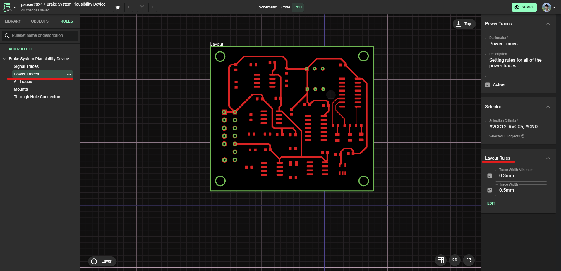
Let's create a selector-based rule setting a trace width of 2mm for a series of different power nets.
Go to the rules tab on the right, add a ruleset, and then navigate to the Selector box located in the inspector panel on the right
You have two options for selecting power nets:
Beforehand, set the names of your power nets to something distinct. For example,
PWR1, PWR2, and so on. Then, for your new rule, select all power nets by inputting:#PWR1, #PWR2into the selector inputAnother method: beforehand, add a
PWRproperty set toTRUEfor all necessary nets. Then automatically select them with a selector input of:[PWR*=TRUE]
Add a
trace widthrule set to 5 mm
For more examples, see the selector-based rules document.
When to use Object-Specific vs. Selector-Based Rules
Selector-based rules are very capable, and it is a good idea to use them over object-specific rules whenever possible. Selector-based rules are all in a single list and have clear targets, such that any collaborators can see why the board is designed in the way it is.
In other words, using selector-based rules makes it easy for users to return to a PCB project after some time and understand why the net widths, clearance values, pad sizes, etc. were designed as they were —making it also easy to see all the rules in the design.
Examples where selector-based rules shine include:
Setting trace widths for all power nets and related vias
Setting keep out values for all capacitors, resistors, and vias
Setting trace widths for all digital signals or a complete netlist
Other components and integrated circuits that may be highly used on the board multiple times
Object-specific rules are great for individual components that require special consideration, that there may be few of on the board. For example, object-specific rules may be useful for:
Setting keep out values for a single microcontroller or other integrated circuit
Removing ground planes under an antenna
An individual net that requires especially large current draw
Individual drill holes in specified locations
Other components that require special care
Advanced Layout Rules Concepts
Layout Rules Inheritance
The concept of inheritance is another crucial aspect of layout rules. In the object tree, you'll notice objects are arranged in a hierarchy. For example, all traces have a parent net, and all components have a footprint that includes silkscreen and pad objects.

Through the concept of inheritance, in applying a rule to any object in the hierarchy, the rule will be applied to all subsequent objects below it.
For example, it is possible to set the width of an individual trace by selecting it in the object tree and applying a rule. However, that will only apply to a single trace.
Instead, if the rule was applied to a net with multiple traces under it in the hierarchy, the rule will automatically be applied to all of these traces –this is known as inheritance.
Layout Rules Precedence
In cases where more than one conflicting rule is applied to an object in your PCB, Flux uses the concept of cascading rules and specificity.
Cascading means that the order of rules matters; when two rules apply that have equal specificity, the one that comes last is the one that will be used
Specificity is a weight that is applied to a given PCB layout rule set when the same element is targeted by multiple rules
Keyboard Shortcuts for Working with Rules
To speed up your workflow when working with layout rules, consider using these keyboard shortcuts:
Ctrl + /(or⌘ + /on Mac) - Open the keyboard shortcuts viewerCtrl + C(or⌘ + Con Mac) - Copy selected objectCtrl + Alt + C(or⌘ + ⌥ + Con Mac) - Copy properties from selected objectCtrl + Shift + C(or⌘ + ⇧ + Con Mac) - Copy layout rules from selected objectCtrl + V(or⌘ + Von Mac) - Paste copied object, properties, or rules
For a complete list of keyboard shortcuts, see our Keyboard Shortcuts Reference.
What's Next
Now that you've learned about layout rules in Flux, you might want to explore:
PCB Rules Reference - Comprehensive list of available layout rules
PCB Layout Rule Selectors - Learn more about selector syntax
PCB Editor Reference - Explore the PCB editor interface
Routing Tutorial - Apply your knowledge of rules to PCB routing
Keyboard Shortcuts - Master keyboard shortcuts to speed up your workflow