
Flux is an AI hardware engineer. It places and routes your board with you, and every change follows your layout rules.
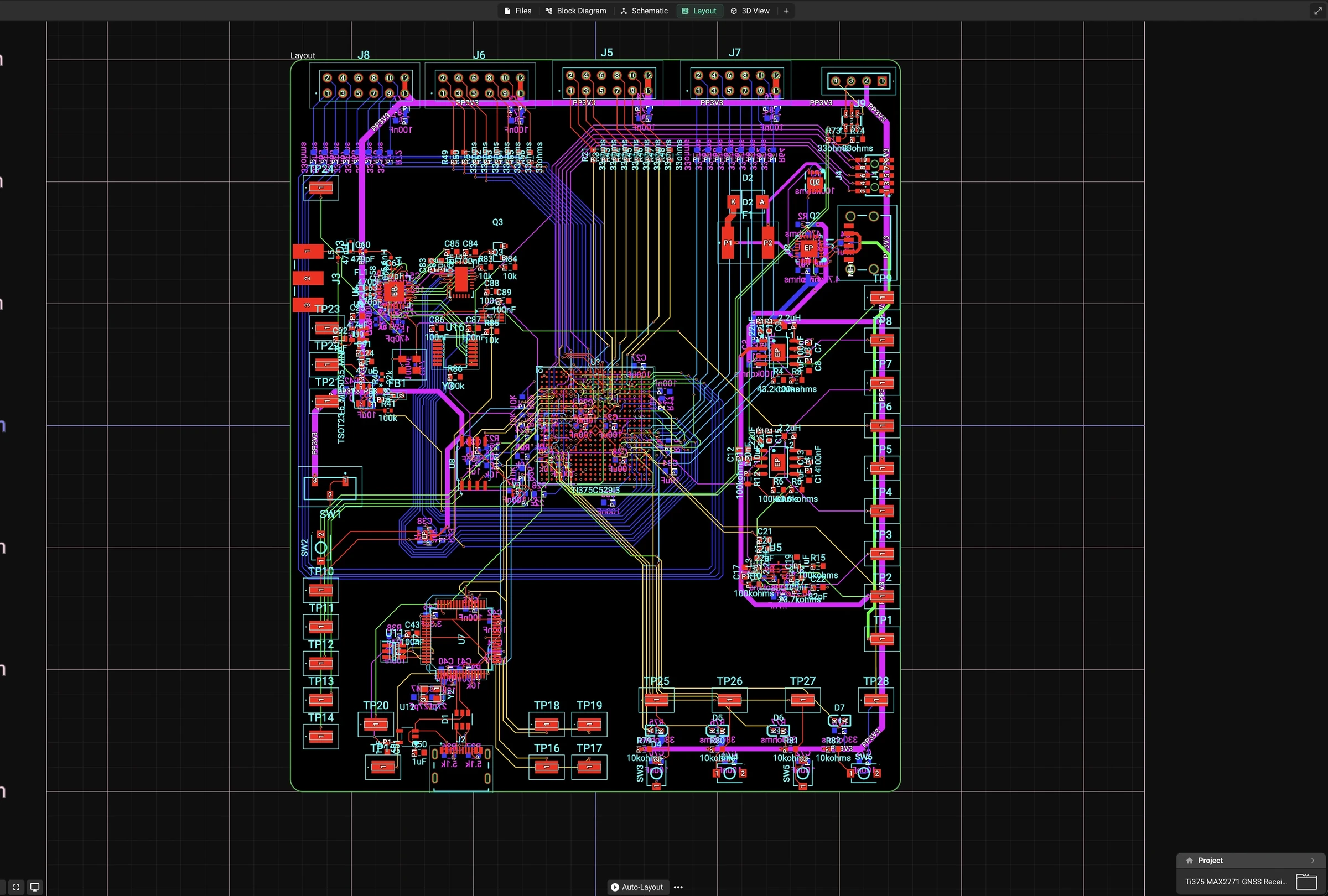
Use the Nets, Components, BOM, Pins, and Knowledge tables to review and edit structured project information.
What is the PCB Editor?
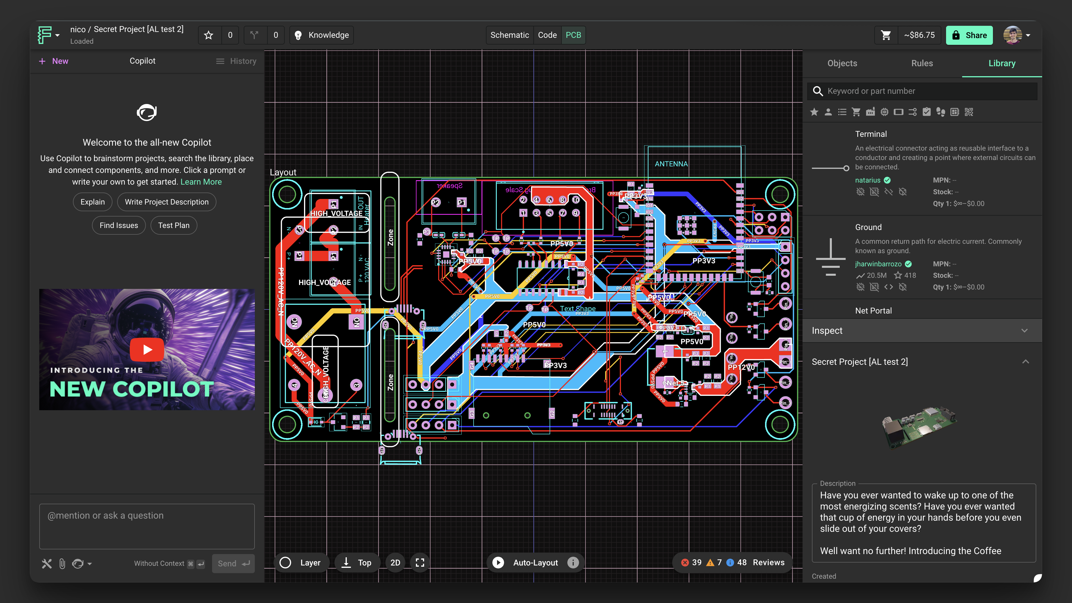
The PCB editor is where you transform your schematic designs into physical circuit board layouts. It stays synchronized with the schematic editor and the 3D view, so you see changes in real time across your design. You can lay out and route the board yourself, or ask Flux to place components and route traces.
The PCB editor is where the schematics come to life. We designed a completely integrated, web-based PCB editor that automatically synchronizes with the Schematic editor and simulator.
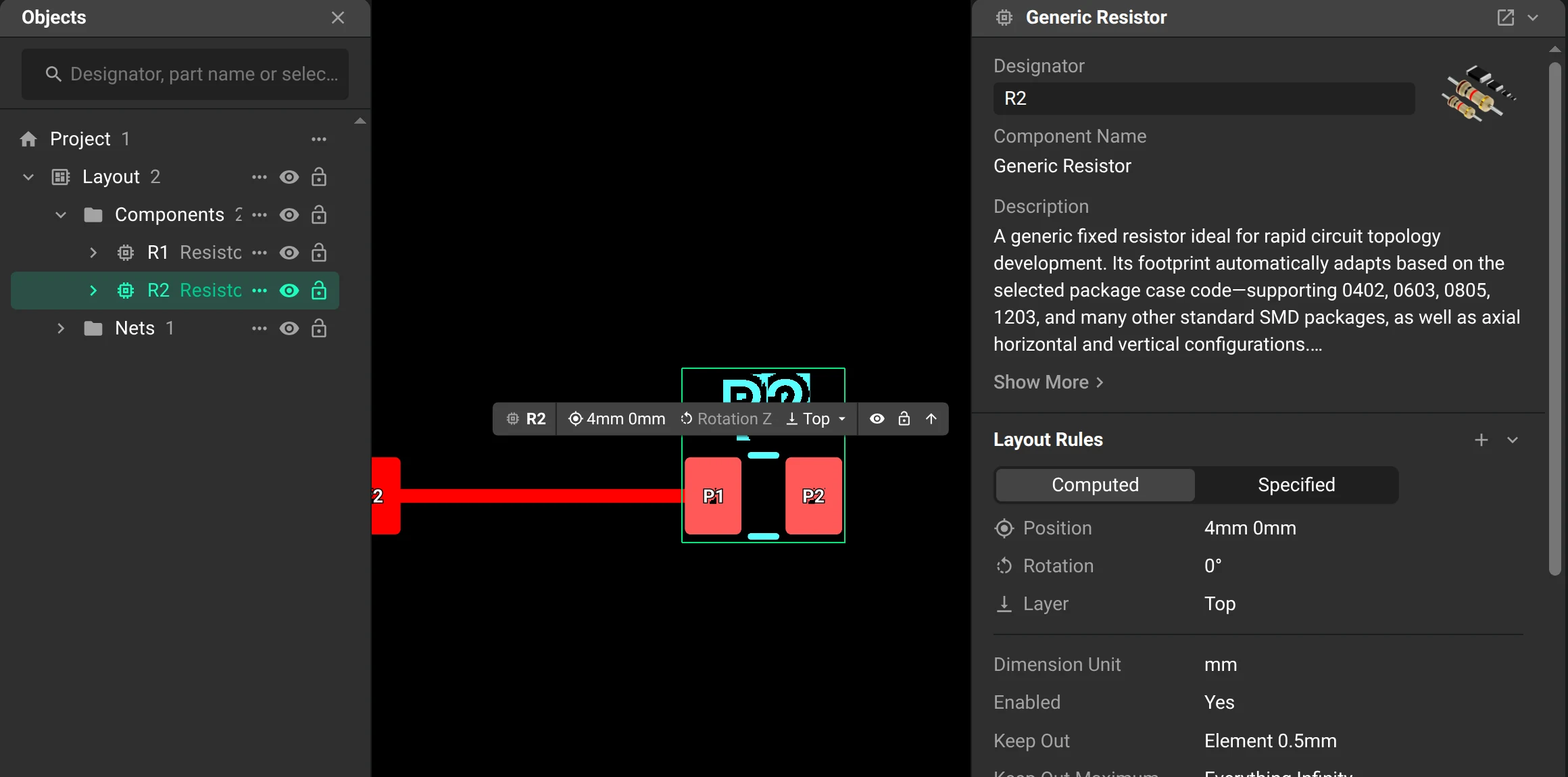
- Layout rules: layout rules that apply to the selected object only.
Key Components of the PCB Editor
The Object Tree
The Object Tree contains a structured map of all the elements present in the PCB editor, from parts to nets to traces. This hierarchical view helps you navigate and manage complex designs efficiently.
Inspector
The Layout Inspector panel on the right side shows contextual information about the selected object. When nothing is selected, the inspector shows document-level information like the description, layout rules, and other properties. When a part is selected, it shows contextual information about it.
The Layout Inspector includes several important sections:
Properties: Carry additional part metadata like Manufacturer part number, value, etc.
Pricing and Availability: Flux automatically searches for pricing and availability in parts with an MPN.
Layout Rules: Contains object-specific layout rules. To learn the difference between selector-based and object-specific layout rules, see Layout Rules Reference.
Select objects
Select objects with the mouse and keyboard on the canvas, or in the Object Tree in the left panel.
Select on the canvas
To select an object, click any of its visible parts. After you select the object, you can drag it from anywhere inside its bounding box.

To select multiple objects, left-click and drag.

Use these keyboard shortcuts for more selection modes:
Shift + left-click: select multiple objects one by one.
Cmd/Ctrl + left-click: deep-select. Select the individual elements that make up the object.
Select in the Object Tree
Click the object name to select it. Multiple selection also works in the Object Tree. Use Shift + click to select the full list or Cmd/Ctrl + click to select multiple individual objects.

Board cutouts
A board cutout is a routed opening through every layer of the board. Use cutouts for connector clearance, display openings, and cable pass-throughs.
Ask Flux to add the opening. Give its shape, dimensions, and position.
To add a cutout in the PCB editor:
Open the Layout tab.
Select the board, then right-click the PCB canvas and select Add → Cutout.
Select the cutout to edit its properties.
Set the shape, dimensions, position, rotation, and corner radius.
Property | What you set |
|---|---|
Position | The X and Y location of the opening. |
Size | The X and Y dimensions of the opening. |
Cutout Shape | A rectangular or circular opening. |
Rotation Z | The rotation of the opening in the board plane. The inspector labels this rule Rotation. |
Corner Radius | The radius of the corners of a rectangular opening. |
Select the cutout on the canvas or in the Object Tree. Drag it to move it, or enter its position for an exact location.
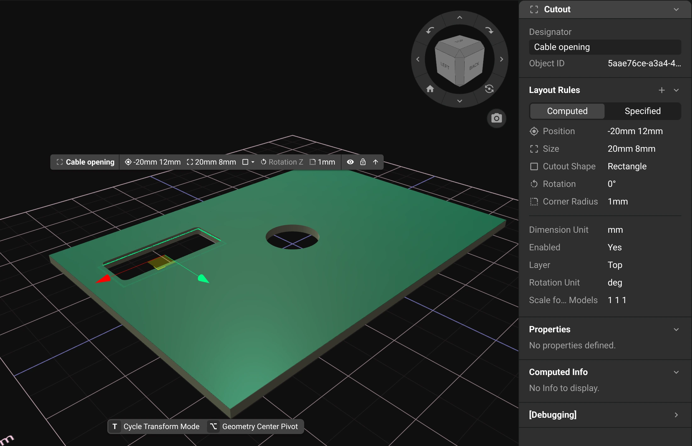
Use a cutout for a routed opening. Use a pad-based mounting hole for a screw, alignment pin, or other drilled hole.
How cutouts carry through
Copper fills keep board-edge clearance around the cutout. See Copper Fills.
The 3D view and the 3D and STEP board models show the opening.
Manufacturing exports carry the cutout in the board outline.
Autorouting keeps traces and vias out of the opening.
Placement checks flag parts that overlap a cutout. A part can occupy the cutout defined in its own footprint.
Show and hide layers
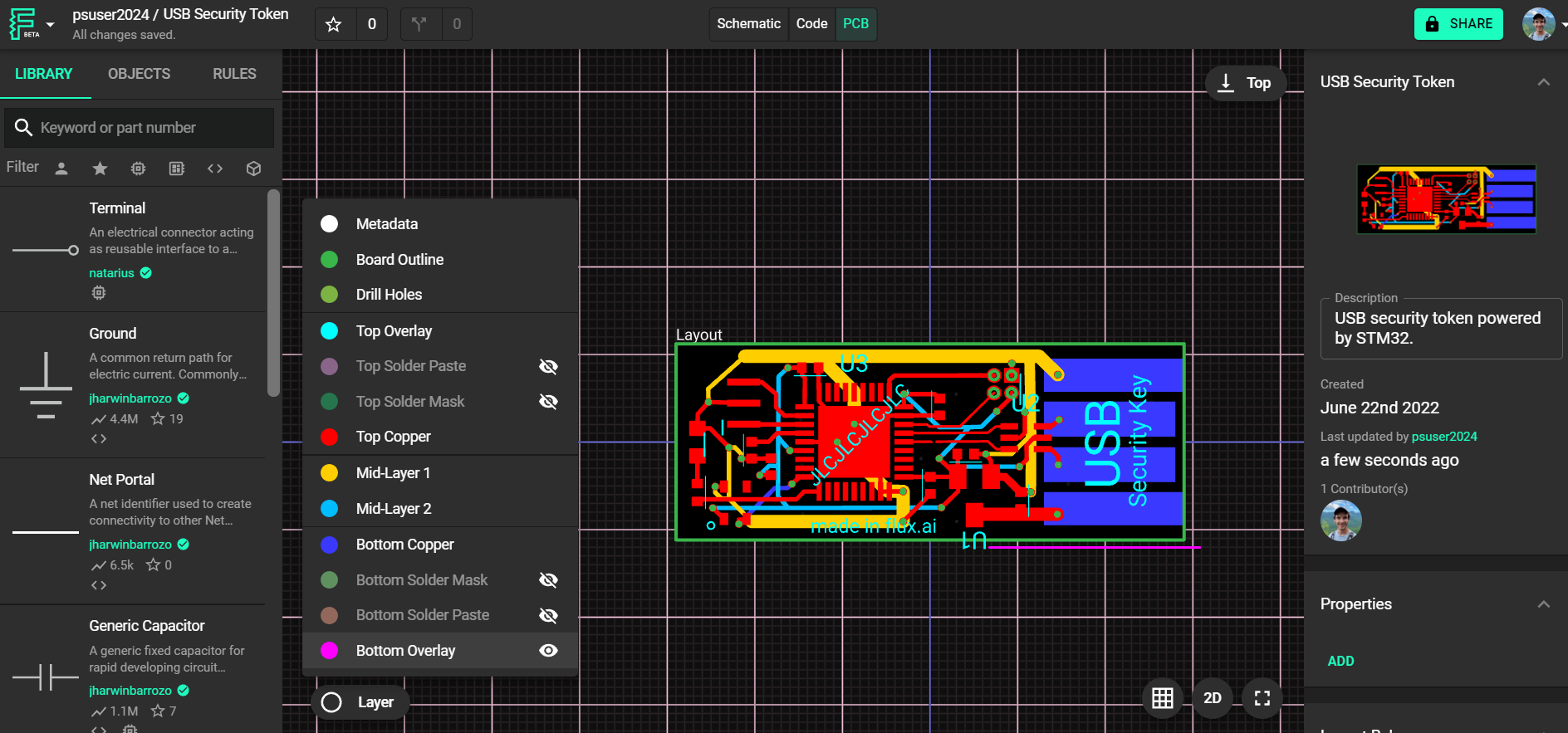
In the 2D PCB editor, you choose which layers are visible, such as signal layers, silkscreen, solder mask, or copper fills.
To show or hide layers in the PCB editor:
Click the Layers icon in the lower-left corner of the canvas.
A panel opens and shows all layers and metadata in your PCB stackup.
Click the eye icon to show or hide each layer.
For layers with copper fills, click the paint drop icon to show or hide the fill.
The 3D view shows a realistic view of your board. In the 3D view, you can:
Rotate, pan, and zoom the board to inspect the overall geometry.
See stacked vias, components, and the general board structure.
Check the copper pours and the silkscreen placement.