Search
Learn how to use the different kind of vias (blind, buried, micro and through-hole) to connect traces across multiple layers.
Overview
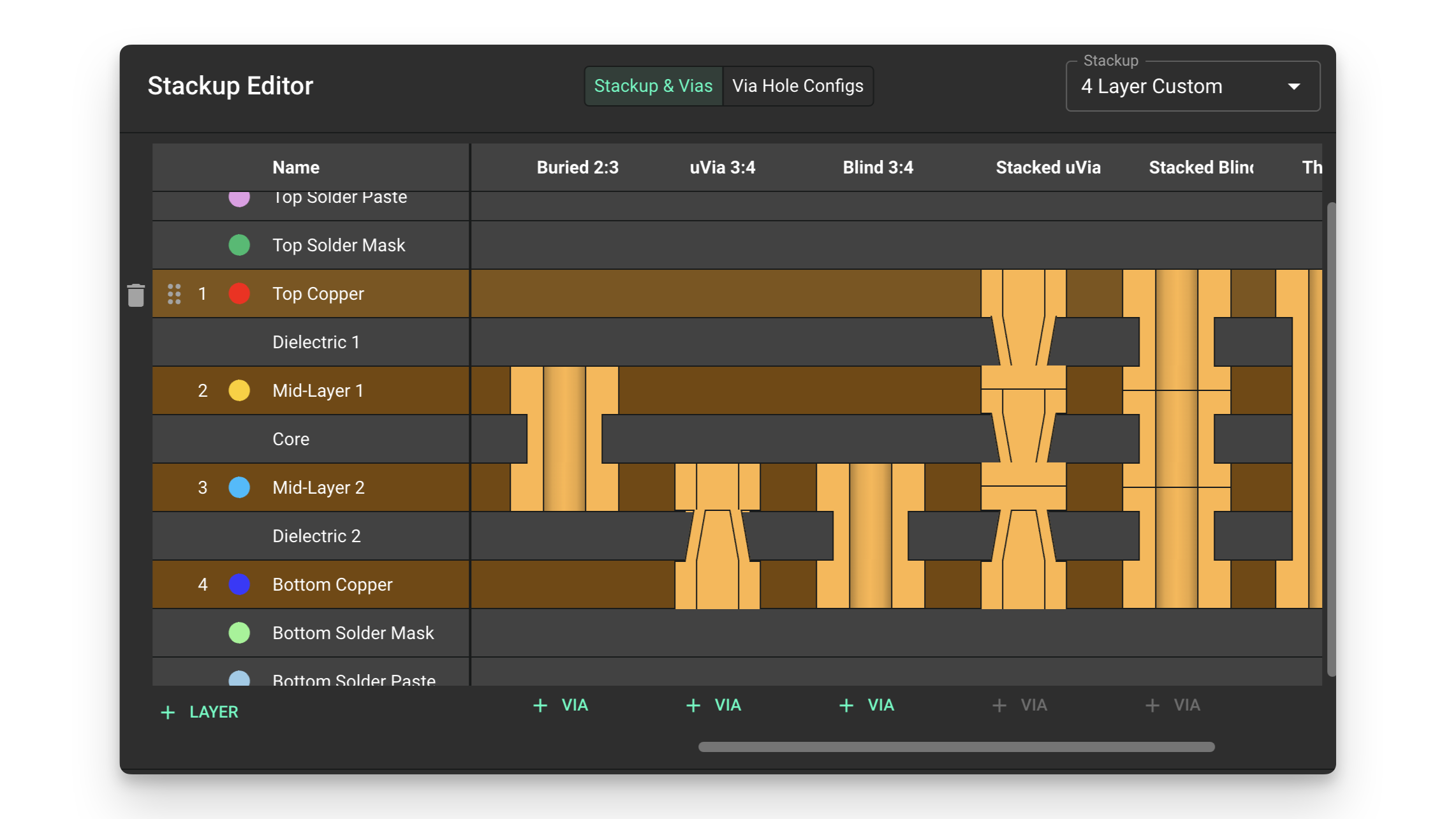
Vias are conductive connections that allow signals to pass between different layers of a PCB. Here's a short overview of the different via types:
- Through vias: Connect the two outer layers (Top and Bottom), and every layer in between
- Blind vias: Connect an outer layer to an inner layer without going all the way through to the other outer layer
- Buried vias: Connect two internal layers without reaching any outer layer
- Microvias: Very small vias typically used to connect adjacent layers
Via Configuration
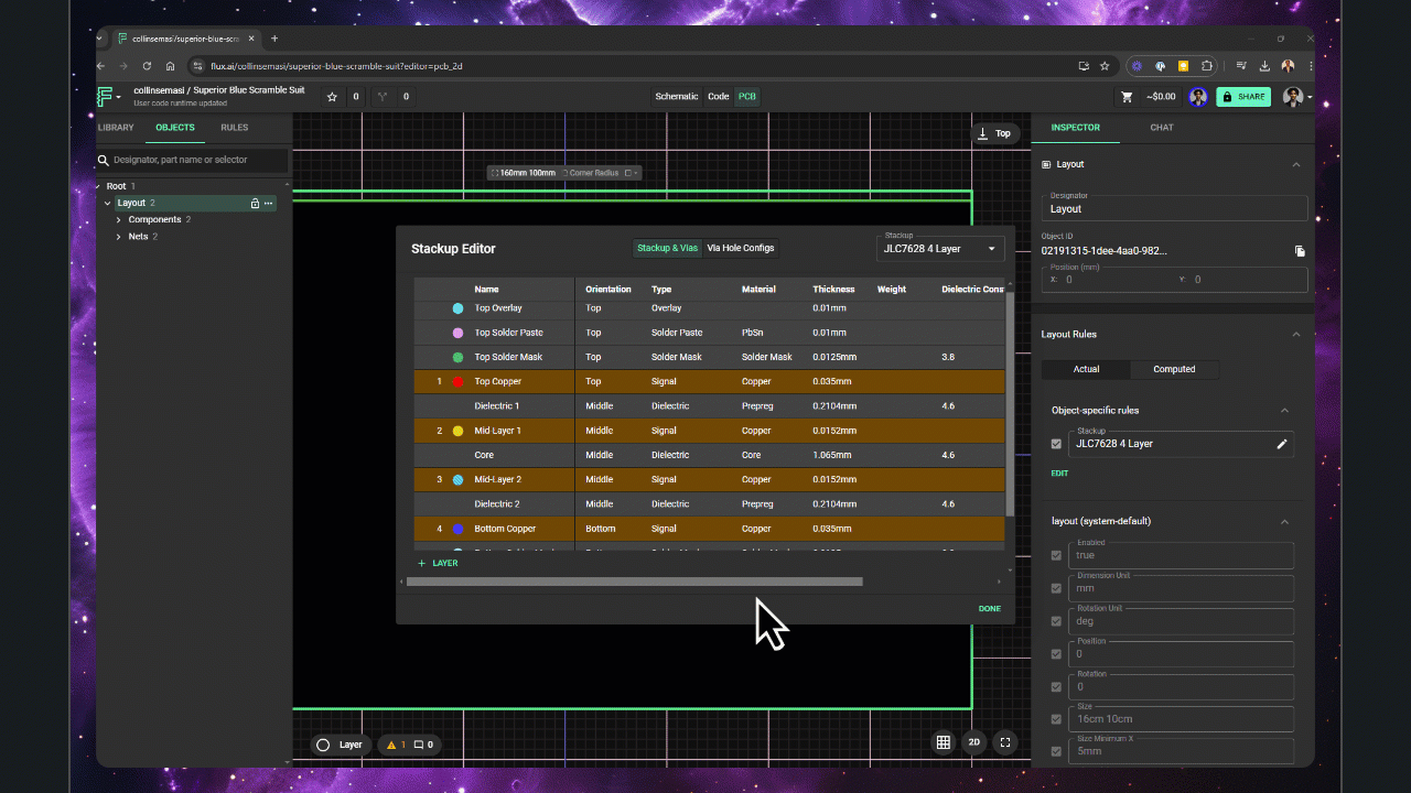
To configure the via types that will be available to route the project you'll need to use the stackup editor:
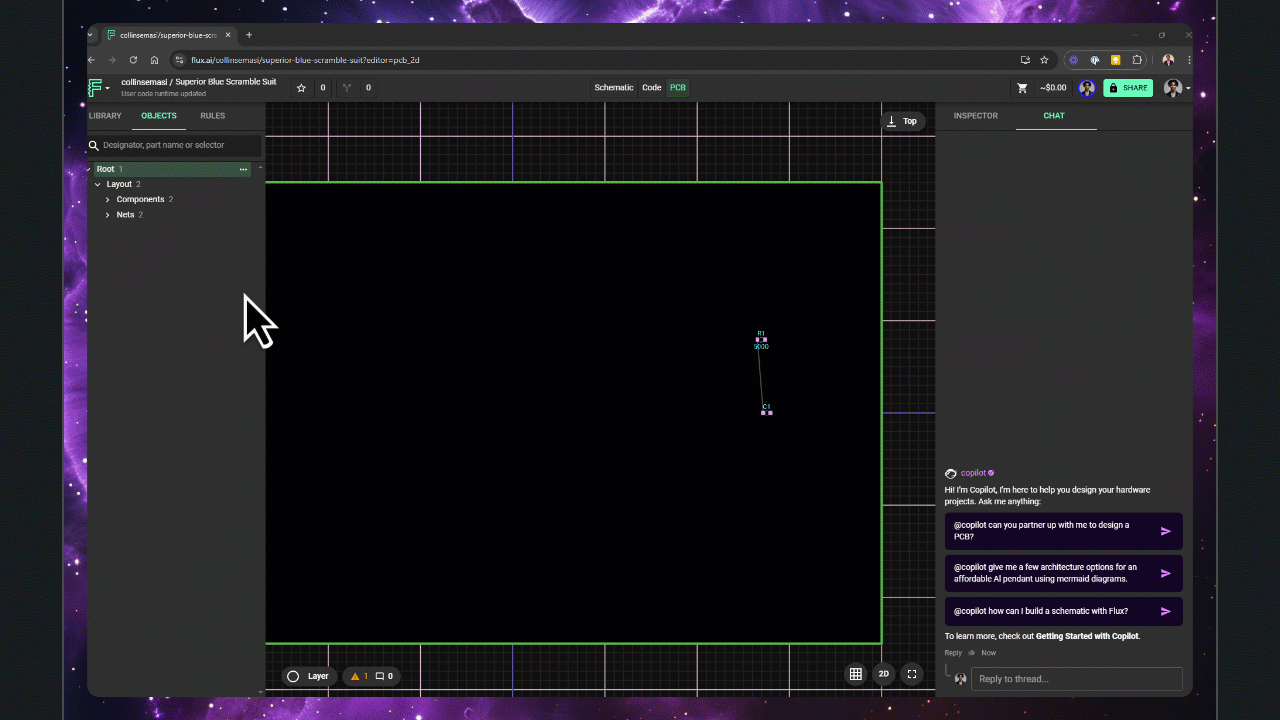
- Select the layout object from the object tree on the left-side panel
- Locate the "object-specific" rules menu on the "Inspector" panel on the right-side
- Add a new Stackup rule
- Click on the pencil icon
Configuring Via Types
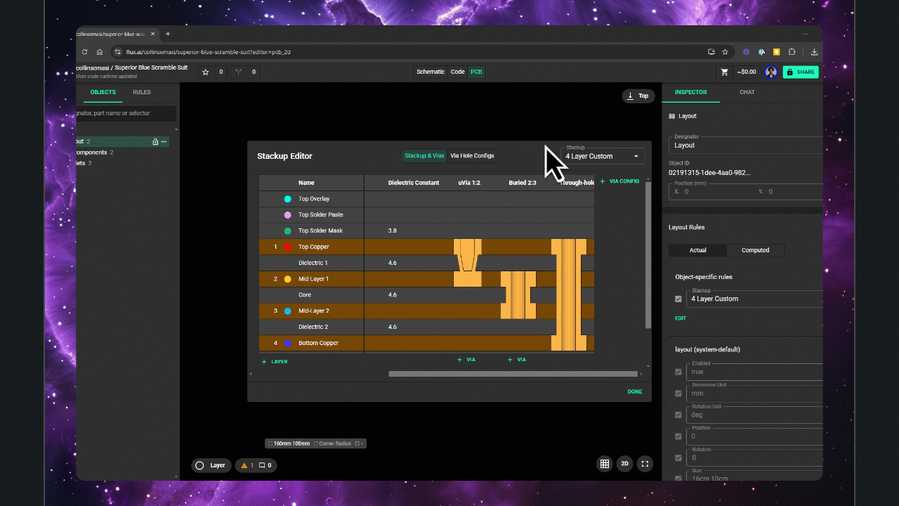
By default, only through-hole vias are configured. To add more via types on the stackup editor:
- Scroll all the way to the right on the stackup editor
- Click on
+ Via Configat the top-right of the stackup editor
- A new Via config column will be created
- You can edit the name of the via type by double-clicking on the column name
- Click on
+ Viaat the bottom of the column to add new vias to the type
- You can click the +Via button as many times as you need to add more vias
- Click to select the newly added via and configure it with the via panel on the right
- Use "Laser Drill" for microvias and "Mechanical Drill" for all the rest of the types
- Hole Size and Size parameters can be typed directly, or configured as a group as mentioned in the next step
Configuring Via Size
You can configure pre-determined via and via hole sizes for quicker via configuration. To add via size configuration groups:
- Navigate to the "Via Hole Configs" tab within the stackup editor
- Modify the default "Mechanical Drill" group, or add a new group by clicking the "+Via Hole Config" button on the bottom-left corner of the editor
- The configured groups will be visible when configuring a via on the "Stackup and Vias" tab
What's Next
Now that you understand how to configure and use vias in Flux, you might want to explore:
- PCB Routing Tutorial - Learn how to route your PCB using vias for layer transitions
- Stackup Editor - Understand how to configure your PCB layer stackup
- Smart Vias - Learn about advanced via features in Flux
- Layout Rules Reference - Understand how to use rules to control your PCB design
Was this page helpful?