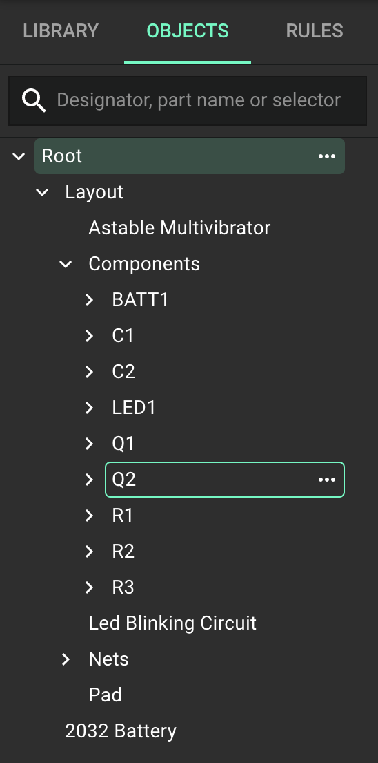
The object tree provides a hierarchical view of all elements in your PCB design, making it easier to navigate, select, and manage complex layouts.
Overview
The PCB editor's object tree contains a comprehensive list of all elements present in your design, organized by their object types. This hierarchical structure helps you:
Navigate complex designs with many components
Select specific elements for editing
Group related objects for bulk operations
Manage visibility of different design elements
Understand the relationships between objects
Object Tree Structure
The object tree organizes PCB elements into logical categories based on their type and function:
Top-Level Categories
Layout: The main PCB board outline and properties
Components: All placed components, organized alphabetically by designator
Nets: Electrical connections between components
Traces: Physical copper connections on the board
Vias: Connections between different PCB layers
Text: Annotations and labels on the board
Shapes: Non-electrical geometric elements
Images: Imported graphics and logos
Rules: Design constraints applied to the layout
Hierarchical Organization
Elements within each category may have their own sub-elements. For example:
A component contains pads, silkscreen elements, and other features
A net contains all traces, vias, and pads connected to that net
Rules may have sub-rules for specific object types
Working with the Object Tree
Navigation
Click on any category to expand or collapse it
Use the search field at the top to find specific objects by name
Right-click on the tree background for additional view options
Selection
Click on any object in the tree to select it in the PCB editor
Hold Shift to select multiple consecutive objects
Hold Ctrl (or Cmd on Mac) to select multiple non-consecutive objects
Right-click on an object for a context menu of actions
Visibility Control
Click the eye icon next to any object to toggle its visibility
Use the visibility controls at the top of the tree to show/hide entire categories
Right-click and select "Hide Others" to focus on specific elements
Organization
Drag and drop objects to reorder them within their categories
Group related objects by selecting them and using the "Group" command
Use tags to create custom organizational schemes
Practical Applications
Troubleshooting: Quickly locate and inspect problematic nets or components
Design Review: Systematically check each category of objects
Complex Editing: Select related objects across different categories
Documentation: Generate reports based on the object hierarchy
Troubleshooting Common Issues
Objects Not Appearing in Tree
Issue: Components or other elements don't show up in the object tree
Solution: Check if filters are applied or if the object type is hidden
Selection Difficulties
Issue: Selecting objects in the tree doesn't highlight them in the editor
Solution: Ensure the correct layer is visible and zoom level is appropriate
Tree Performance
Issue: Object tree becomes slow with very large designs
Solution: Collapse unused categories and use search to find specific objects
What's Next
Now that you understand the PCB layout object tree, you might want to explore:
Object Types Reference - Learn about the different types of objects in Flux
PCB Editor Reference - Master the PCB editor interface
Layout Rules - Understand how to apply rules to objects
Component Placement - Learn best practices for organizing components