Polygons allow you to create custom copper shapes that are tied to specific nets. This reference guide covers the key aspects of working with polygons in your PCB designs.
For step-by-step instructions on creating and editing polygons, see the Working with Polygons tutorial.
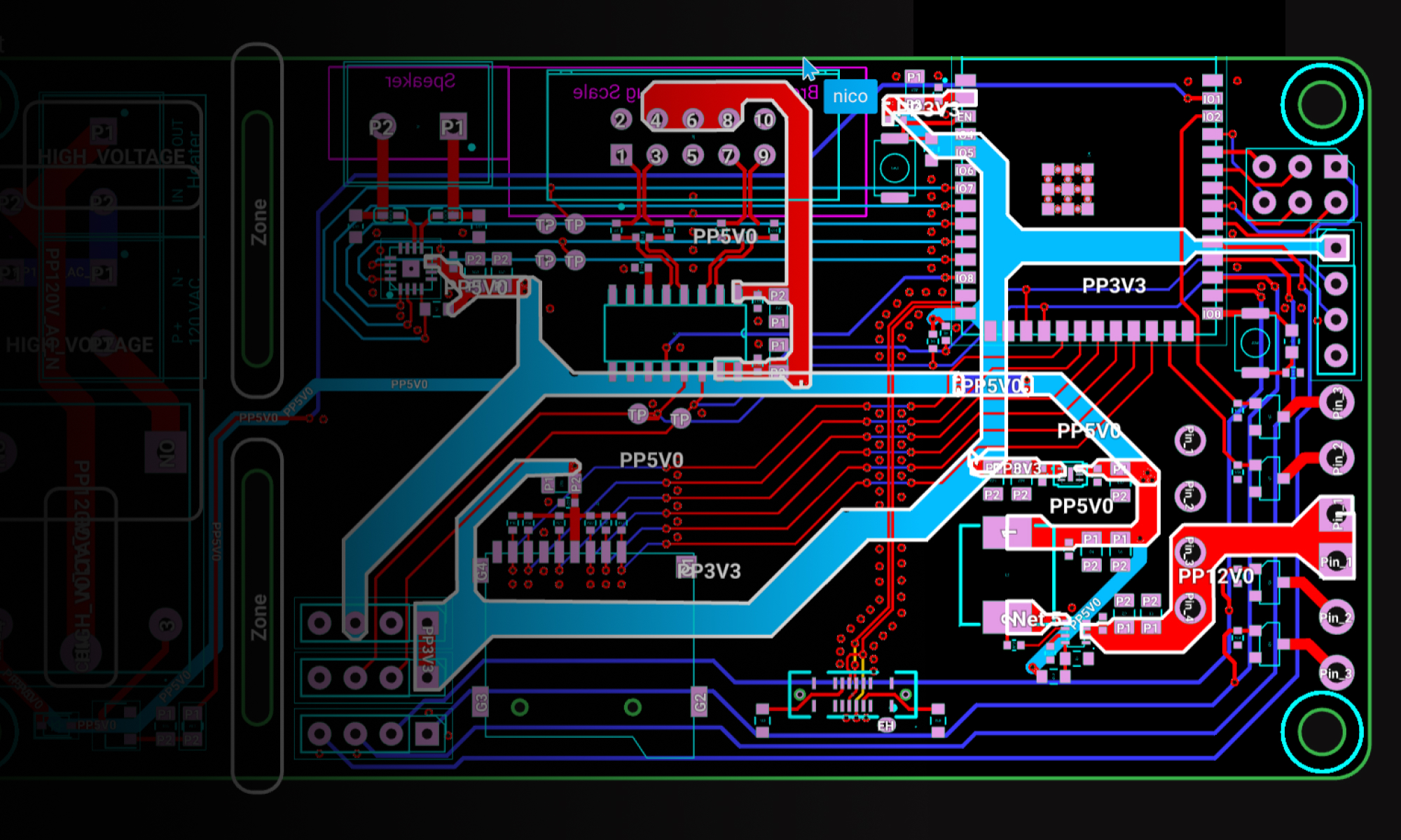
Polygon Rules
The following rules can be configured for polygons in the Inspector panel:
Rule | Description |
|---|---|
The shape of the polygon, defined using SVG path syntax. | |
The copper layers the polygon appears on | |
Determines the minimum feature size for the polygon | |
Controls the density of via stitching if applied | |
Controls the offset of via stitching if applied | |
Prevents copper pour in specified areas |
Polygon Hierarchy and Priority
When multiple polygons overlap, Flux uses a size-based priority system to determine which polygon takes precedence:
All polygons take priority over Copper fills
Smaller polygons take priority over larger polygons
Polygons of the same net will merge unless they have different properties
This automatic priority system allows you to:
Create complex copper structures with cutouts by using smaller polygons
Implement split planes for different power domains
Design sophisticated RF structures with controlled impedance
Create thermal relief patterns around component pads