
Control what layers you see in the PCB editor.
Overview
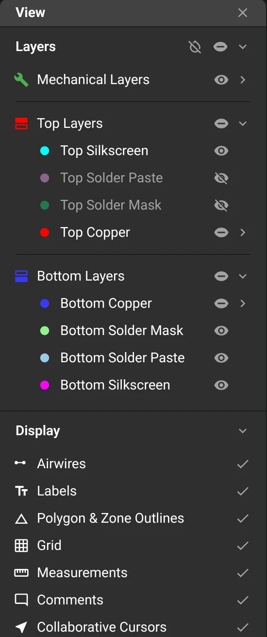
In the 2D PCB editor, you choose which layers are visible, such as signal layers, silkscreen, solder mask, or copper fills.
Use layer visibility controls in the 2D PCB view.
Getting Started
To show or hide layers in the PCB editor:
Click the Layers icon in the lower-left corner of the canvas.
A panel will open showing all layers and metadata in your PCB stackup.
Use the eye icon to toggle visibility for each layer.
To show or hide the fills on one copper layer, expand the layer and click the eye icon on its Fills row.
Copper Fill Visibility
Copper fills are visible by default. Open the View panel, expand Layers, and click Hide All Fills in the section header to hide all copper fills. Click Show All Fills to show them again.
To show or hide the fills on one copper layer, expand the layer in Layers and click the eye icon on its Fills row.
Press H then F to toggle all copper fills on Windows, Linux, and Mac. Press the keys in sequence, without modifier keys. These controls change visibility, not the net's Connected Layers rule. See Copper Fills.
Stackup areas
On a flex or rigid-flex board, the PCB editor shades each Stackup Area and shows its name and area stackup. To show or hide this overlay, open the View panel and use Stackup areas. See Flex and Rigid-Flex Boards.
What About 3D View?
The 3D PCB view provides a high-level, realistic visualization of your board:
What You Can Do in 3D View:
Rotate, pan, and zoom the board to inspect the overall geometry.
See stacked vias, components, and general board structure.
Visually confirm copper pours and silkscreen placement.