Getting Started in Flux: PCB Layout & Routing Guide
Before Watching
Watch "PCB Design Tutorial Part 1" and "PCB Design Tutorial Part 2" for the setup and schematic.
Overview
In this tutorial, we'll cover:
- PCB layout discussion tips
- Part Placement
- Routing and associated routing tips
- Final touch ups: board size, removing silk, mounting holes
- Final Design Rules Check (DRC)
- Replacing the original potentiometer for a digital potentiometer with the buck converter
- Replacing the physical switch with an ESP32 to control both the digital potentiometer and the buck converter. This will allow us to to control the board with a wifi trigger event such as a meeting start or phone being set to do-not-disturb
Part Placement Intro
The first step of the PCB layout is part placement. Let's start doing the pcb for the buck converter module first.
- Go to the PCB tab of the Buck converter module
- Here, parts can be dragged, rotated, and flipped on the PCB canvas or selected directly on the Objects tree
- Select all components and press F to place them all in the bottom layer
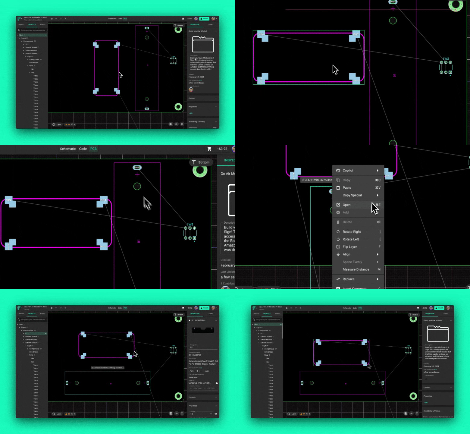
- To flip the viewpoint, click to Top button located in the top right so we can lay out the board from the bottom
To move a component, left-click on it and drag it to the desired position. For rotating a part, there are two options:
- Right-click on the part you want to rotate and select "Rotate right" or "Rotate Left"
- To rotate parts quickly, use the open or close square brackets
[ ]
Your layout will then look something like this:
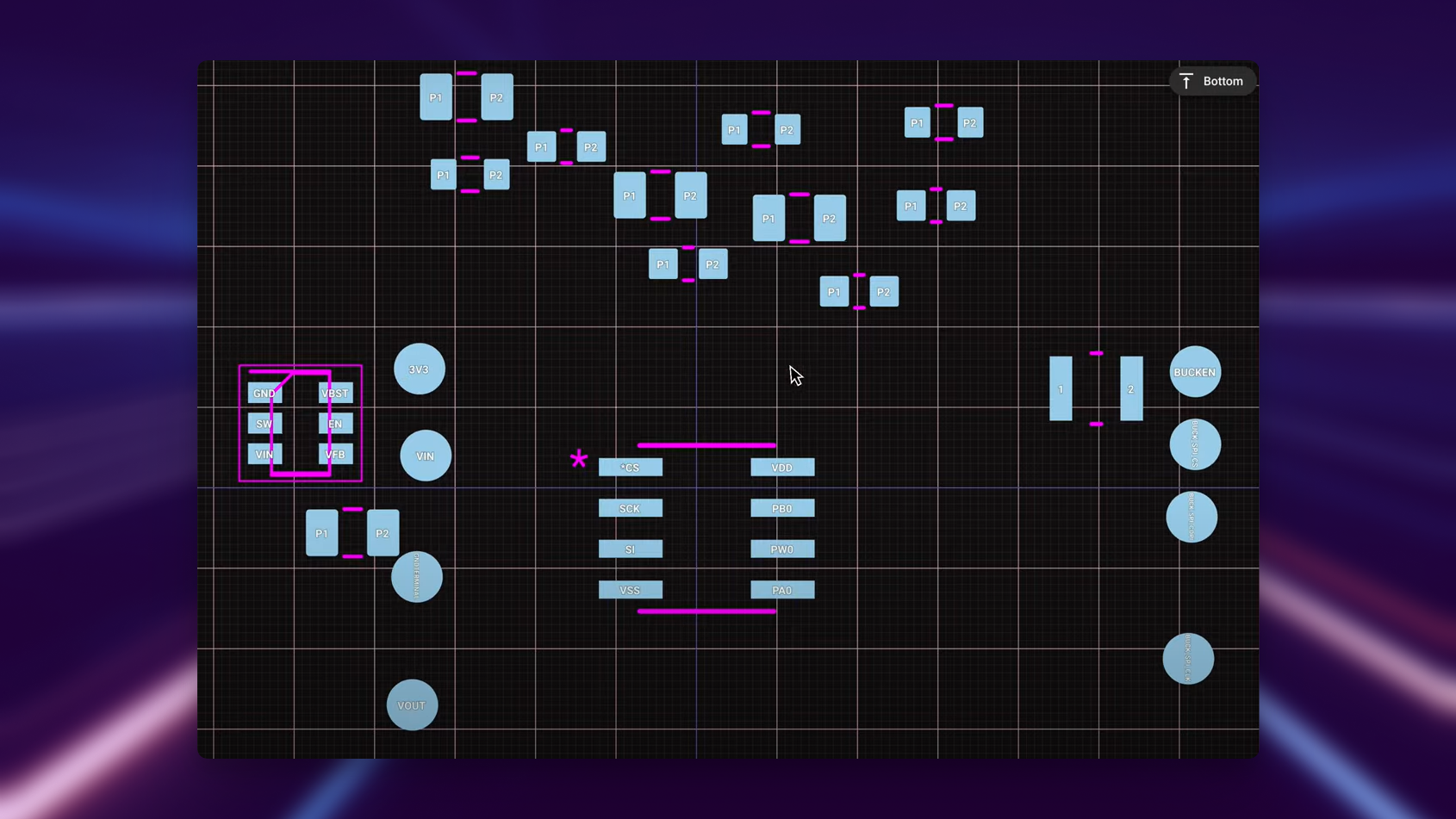
Aligning Parts
If there's a series of components you'd like aligned in a specific way, see below.
- Select the components > right click > Align > Align Top.
- You can also space them evenly in the right-click menu.
- Shift + drag to move objects on a straight axis.
To center the letters about the X-axis, you can add an object-specific rule.
- Click edit on the Layout rule on the right in the inspector panel.
- Add rule for Position Y and set it to 0 on the first letter 'O'.
- Then, copy the layout rule and paste it on other letters
Terminals Pads in the PCB
When you add a terminal it creates a test point object on the PCB to probe it later.
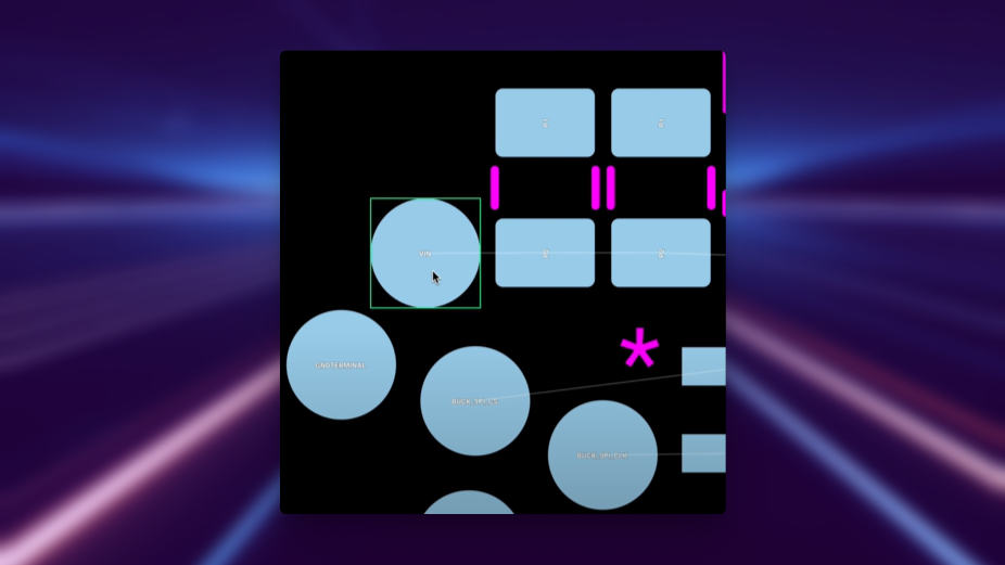
If you want to remove it you can add a property "Exclude from PCB" and set this value to true. This is found in the inspector panel on the right under properties, with the terminal selected.

You're also able to change the size of the test point to make it look smaller as desired by selecting it in the pcb editor and changing the diameter.
Part Placement Process
Go back to PCB, you should see air wires connecting all the parts. In this section we'll be organizing our parts on the board. Generally, it makes sense to follow a similar structure to that of the schematic, in regard to part placements.
- Switch between Schematic and PCB to know what part to place where.
- C1, C2, and C3 should be placed near the Vdd pins.
- Press bracket key [ or ] to rotate any parts
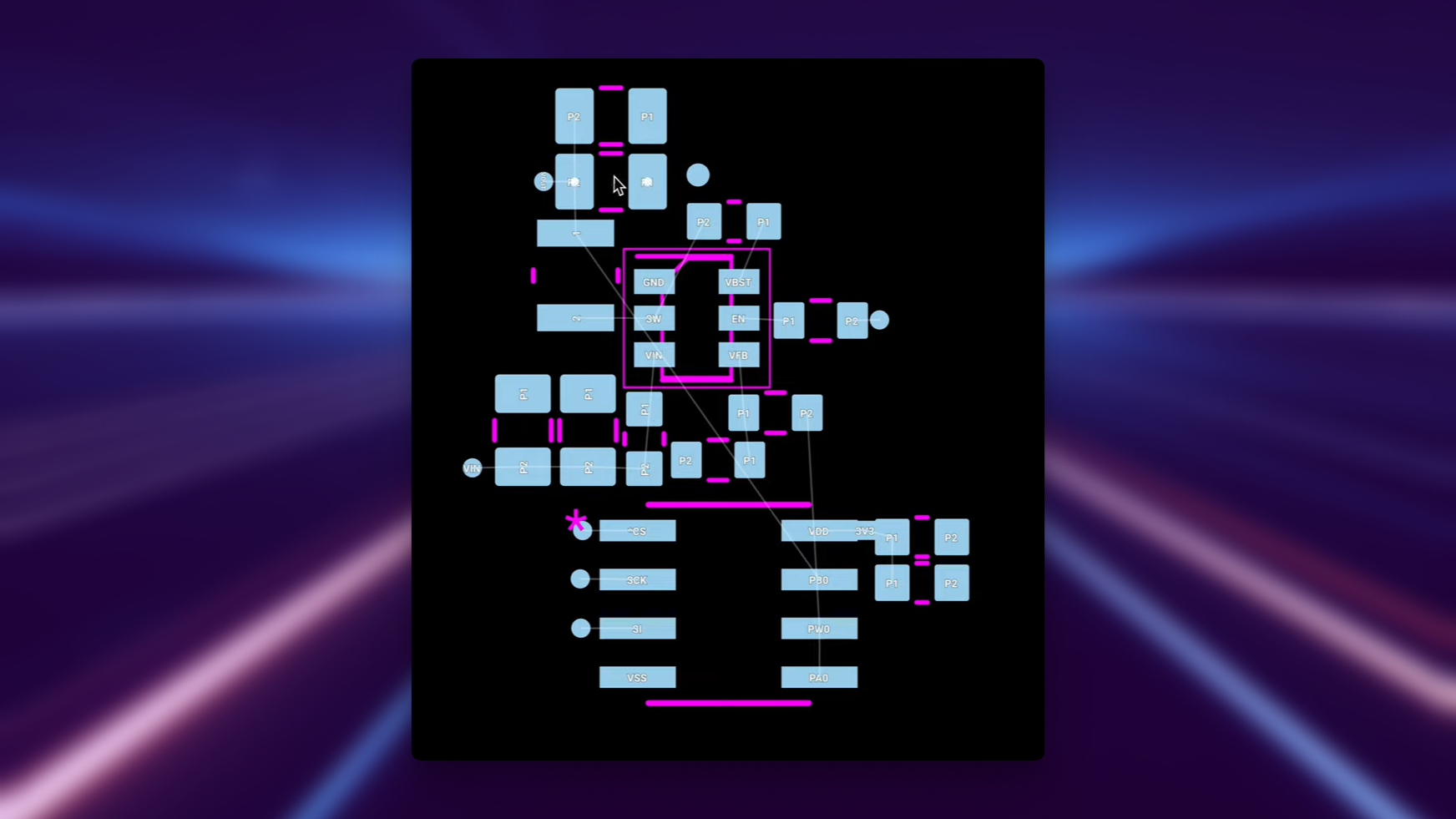
When laying out the buck converter and general IC, you want to place the decoupling capacitors close to the power supply pins to minimize parastic inductance. These inductances counteract the attenuation effect of capacitors at high frequencies. For the same reason, place your lower value capacitors closer to the Vdd pins. In the image below we've placed the decoupling capacitors, highlighted in yellow, close to the Vdd pins.
- To check the value of the pins, click on them and look at the inspector panel on the right
- For spacing, keeping things dense is generally preferred
- If you're unsure about collisions you can always go into the 3D Editor to see
After part placement, our board looks like this. Below is the final layout of the buck converter module. Notice the two capacitors next to the Vdd pin.
Routing Intro
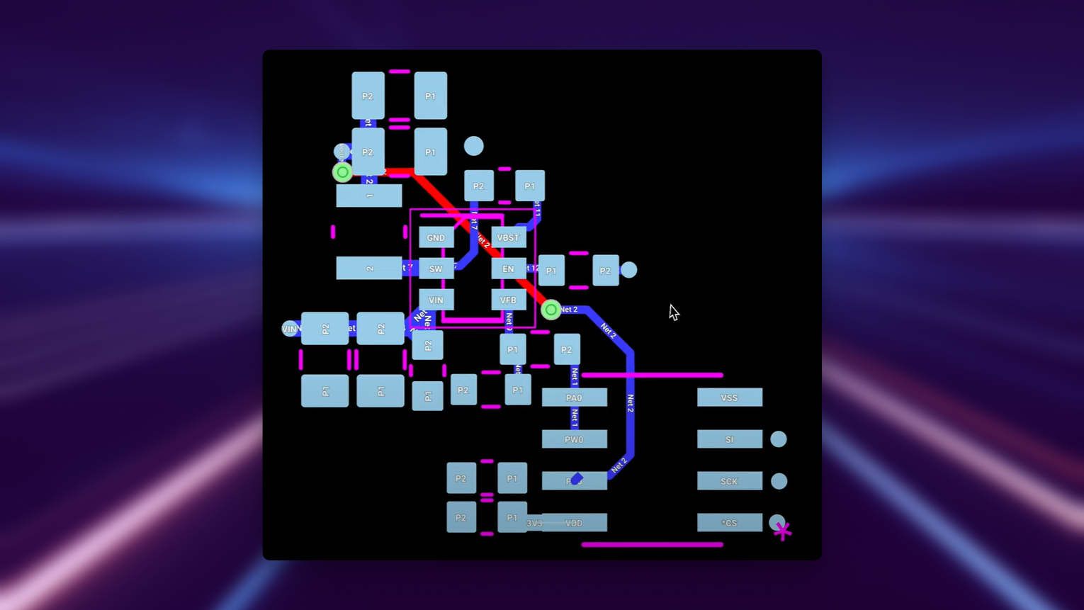
Once we've completed part placement, we can move onto getting rid of the air wires! To start routing, click on a routing touch point and a trace will appear.
- Press F to change the route/trace angle (elbow) direction and W to change the size of traces.
- Connect the components based on the schematic and airwires
As you route, you'll see air wires disappear and be replaced by copper. You can also switch the layer you're routing on by clicking V, to place a via and switch layers. After routing our board looks like so.
- When you finish, publish the changes with
Ctrl+Pand you should see the change in the parent project
Changing Trace Width
For the buck-converter module above, we've routed it all with the same trace width. However, once we return back to our main project, we'll need to know how to change the trace width when routing.
- You can set a Preferred Trace Widths rule for your objects or nets by selecting the Nets object in the objects tree and adding the rule
- Place the trace down and you will see its associated Net container highlighted in the object tree
- You can also use a PCB trace width conversion calculator to find the required trace width
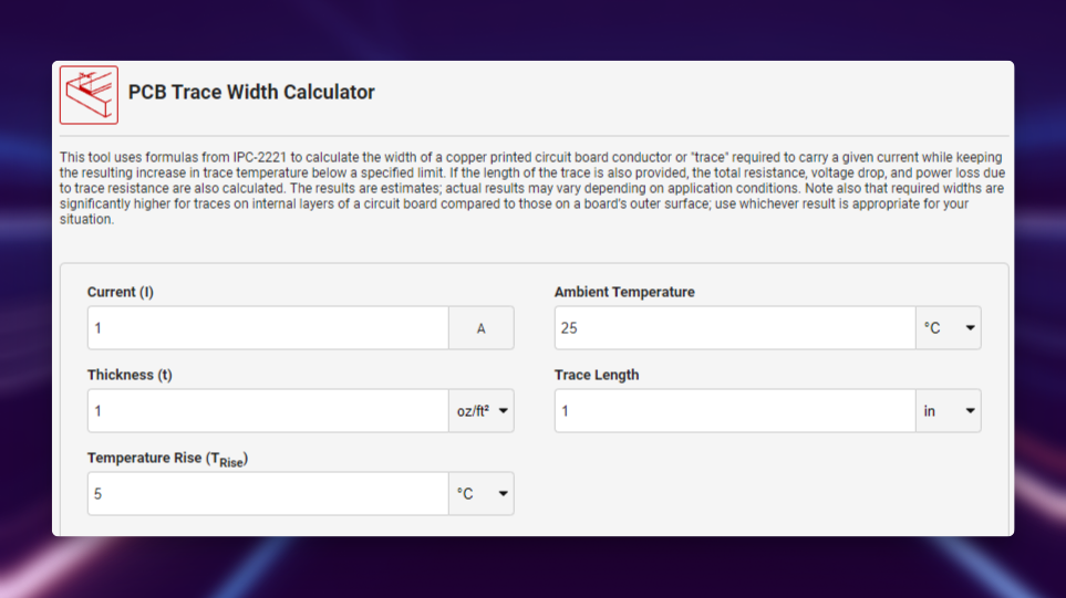
- You can also change trace width by hovering on the trace segment and editing the width on the bar that pops up
- You can add a parent rule on the RULES left panel; use selectors on the right to select the net (ex: #Net27), and add a trace width rule and an !important rule to override.
Impedance Control Routing
Similarly, when routing our main board, we'll have to deal with traces that require impedance controlled routing, such as for USB connectors.
As a general tip for routing, route your high frequency signals first and then move on to power. In general, you want to make sure your most important signals have the cleanest path and the least amount of parasitics.
- The highest priority high-speed signals on this board would be the USB data lines.
- This USB data line works with an impedance matched differential pair signal. To route it, you just begin routing like you would any other trace and notice that two traces will pop out for pair routing.
- Press Ctrl or CMD to toggle pair/single routing.
- You can place your trace segment, right click to switch layers, and place another trace segment to finish your connection. Then you can drag the vias that should have appeared apart with Shift + Drag
The calculated values for this impedance controlled pair can be found in the net container. You can find the the actual and computed properties tab on right panel.
- In order to set up an impedance control traced you have to configure it in your part.
- If you double click the part you can see in its inspector panel that there is a 90 ohm controlled impedance with 15% tolerance.
How to Change Board Size
Now, we can go back to our main project and set the board size.
In Flux you can easily change the basic board shape and size, or even use a custom shape with an SVG or DXF.
- Click on the layout node either in the object tree or in the canvas
- A bar comes up where you can edit the size and shape. You can also change the shape to be rounded, circular, or keep it as rectangular.
With the 'Layout' object selected, you can also add more rules to further modify the board
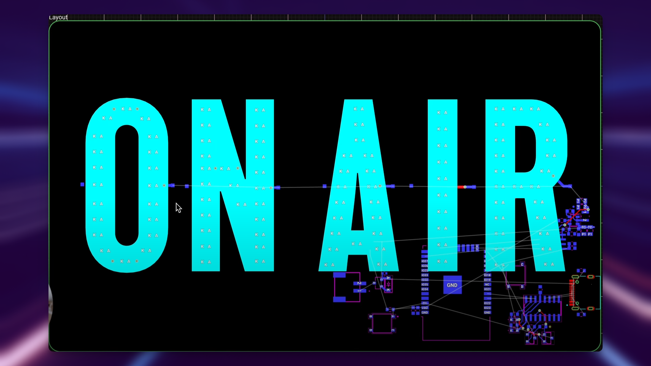
- Add a stackup rule to the object-specific rules, changing it to a 4 layer board.
- Bring your components to the board, press F to flip them to the bottom except the USB connector.
- Finally, organize your components on the board. Here is the layout from the top view.
Copper GND Fills
Toggle the visibility on the layer.

If you want to disable copper fills per layer, you can go into your object tree and under nets, you can find the ground fills.
- Add an object specific rule: Connected Layers and here you can toggle which layers you want them to be connected to (ex: Top layer)
Stitching Vias
To adjust the Stitching vias, go into the Nets section and find the ground layer
- Add an object specific rule: Fill Stitching Density/Offset.
- Set density to 0 to disable stitching vias
RF Copper Cutout
If you're working with an ESP32 or any other RF product you can't keep copper underneath its antenna. For this reason you must add a copper cutout or keepout: go to components, add a cutout pad with the following object specific rules. Notice that connected layers is set to all and the pad-type is set to standard so it is applied to copper and all layers.
After laying out the top-side of the board and routing all connections together:
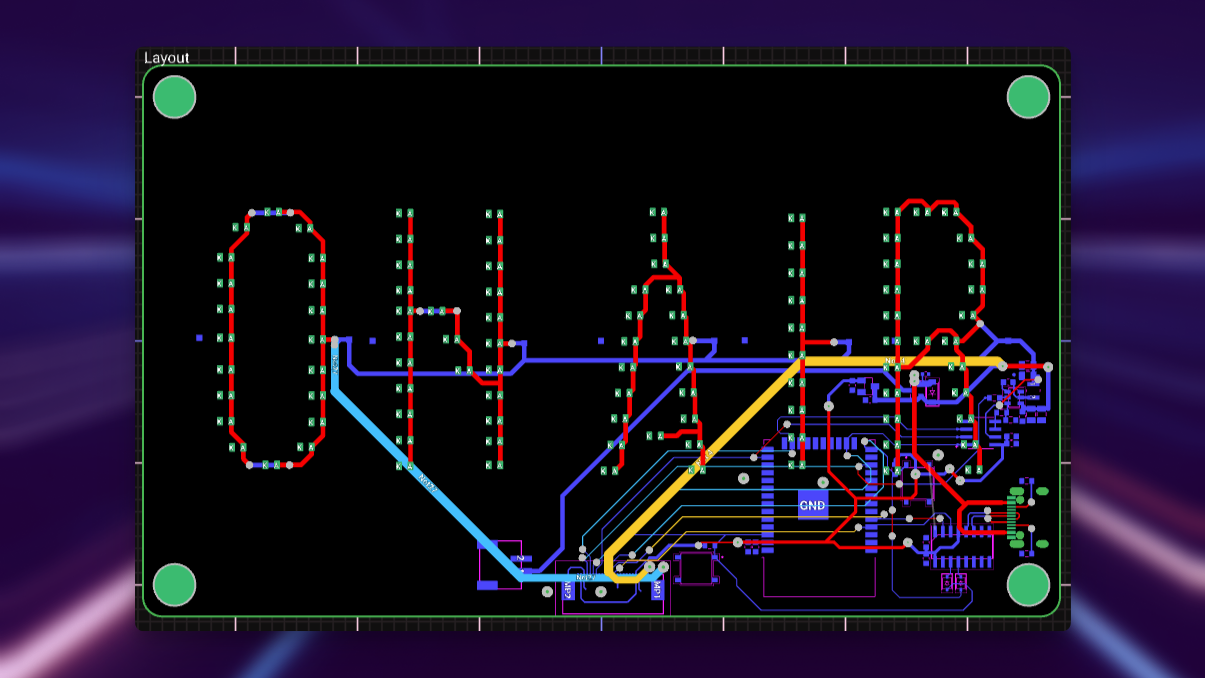
Final board after wiring - top view
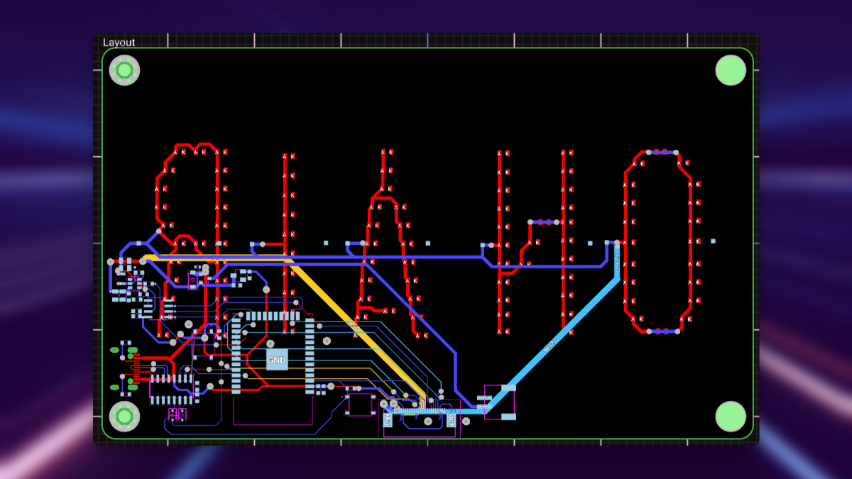
Final board after writing - bottom view
Mounting Holes
In the schematic, search the library for M3 Mounting Holes and place them in the schematic.

This will then sync with the PCB so you can place them in all four corners. You can then set their individual position.

Removing Silkscreen
Sometimes, component density on the board may be too great that having large silkscreen text may reduce visibility or board aesthetic and comprehension. For this reason, it may be desirable to shrink the size or completely remove silkscreen text. An example would be the R10 designator text
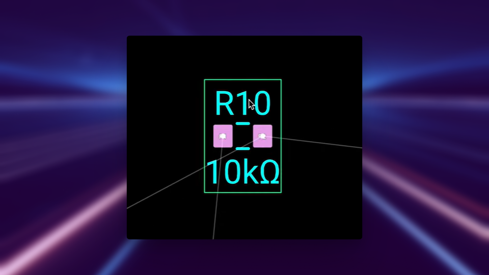
Above we see what it looks like before removing silkscreen.
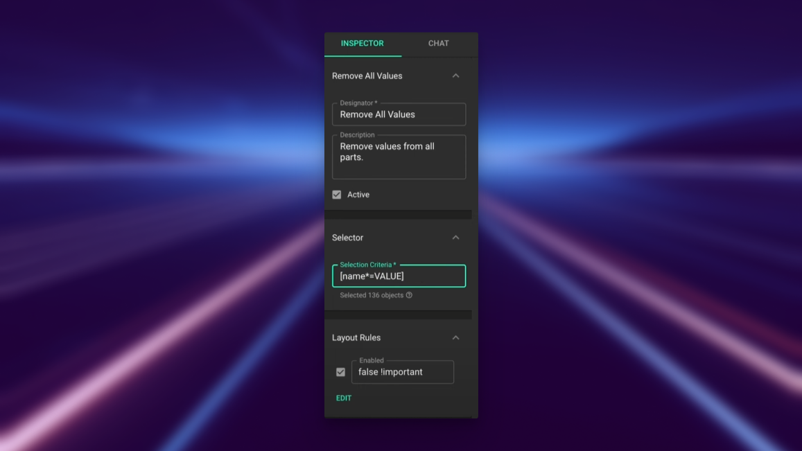
- Switch from the schematic tab to the PCB tab in the top center navigation bar
- Click on the RULES tab on left panel, activate "Hide Designator + Font Size" and "Remove All Values"
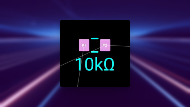
Then we can see that we've removed the silkscreen text as shown below. We can also remove the 10kΩ text as well if we'd like by creating another rule with the selection criteria set to: [name*=VALUE].
Checking For Problems Through the DRC
The layout rules in Flux minimize errors, yet specific issues like overlapping traces, unrouted nets, and absent footprints necessitate extra verification. Flux features real-time Design Rule Checks (DRCs), with outcomes available through the messages menu.
Dealing with DRC errors allow designers to verify that the design adheres to specific manufacturing and performance standards, and are crucial to identify as they can impact manufacturability, reliability, and compliance with industry standards.Before you order the board you want to check for any DRC errors in the problems panel at the bottom.
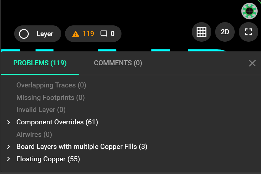
DRC Problems are found at the bar at the bottom of the PCB layout editor canvas.
For this project:
- Ignore component overrides, multiple copper fills, and floating copper warnings
- Important though, is checking the Airwires to see which paths are not connected. Clicking on it will show you on the board where this issue is.
DRC Errors Summarized
Critical DRC errors are summarized below, and in depth in this article.
- Overlapping Traces: A DRC violation occurs when two traces from different nets overlap.
- Floating Copper: Detects unconnected via, trace, or copper fill island to any net, including isolated copper fill islands, floating vias/traces, and requires connection or appropriate stitching vias/keep out rule adjustments for resolution.
- Board Layer with Multiple Copper Fills: Violation occurs when multiple copper fills from different nets are requested on a single layer, contradicting the Connected Layers rule for Net objects.
Troubleshooting Common Issues
Component Placement
- Components not appearing in PCB view: Ensure components have valid footprints assigned in the schematic
- Alignment difficulties: Use the alignment tools (right-click > Align) or keyboard shortcuts for precise alignment
- Component collisions: Check for overlapping components in the 3D view and adjust placement accordingly
Routing Challenges
- Unable to change trace width: Verify that no !important rules are overriding your width settings
- Differential pair routing issues: Make sure the part has proper impedance control settings in its properties
- Via placement problems: Check your stackup configuration and ensure vias are properly sized for your manufacturer
Copper Fill Problems
- Ground fill not appearing: Verify the net is properly connected to ground and the fill is enabled
- Multiple copper fills error: Ensure you're not trying to place different nets' copper fills on the same layer
- Stitching vias not appearing: Check the Fill Stitching Density setting is not set to 0
Design Rule Checks
- Persistent DRC errors: Click on each error in the problems panel to locate and address the specific issue
- Clearance violations: Adjust component placement or trace routing to meet clearance requirements
- Unrouted connections: Check for airwires and complete all necessary connections
What's Next
Now that you've completed the PCB layout and routing, you're ready to move on to:
- Export and Manufacturing - Prepare your design for production
- Ground Fills Deep Dive - Learn more about working with copper fills
- Multi-layer Design - Explore techniques for routing across multiple layers
- Layout Rules Deep Dive - Master Flux's powerful layout rules system
- Design Rule Checks - Understand how to ensure your design meets manufacturing requirements