Control what layers you see in the PCB editor.
Overview
Flux gives you full control over which layers are visible in the 2D PCB editor, helping you focus on exactly the data you need—whether that’s signal layers, silkscreen, soldermask, or copper fills.
Layer visibility controls are only available in the 2D PCB view. The 3D view uses a simplified rendering mode and doesn’t support layer selection.
Getting Started
To show or hide layers in the PCB editor:
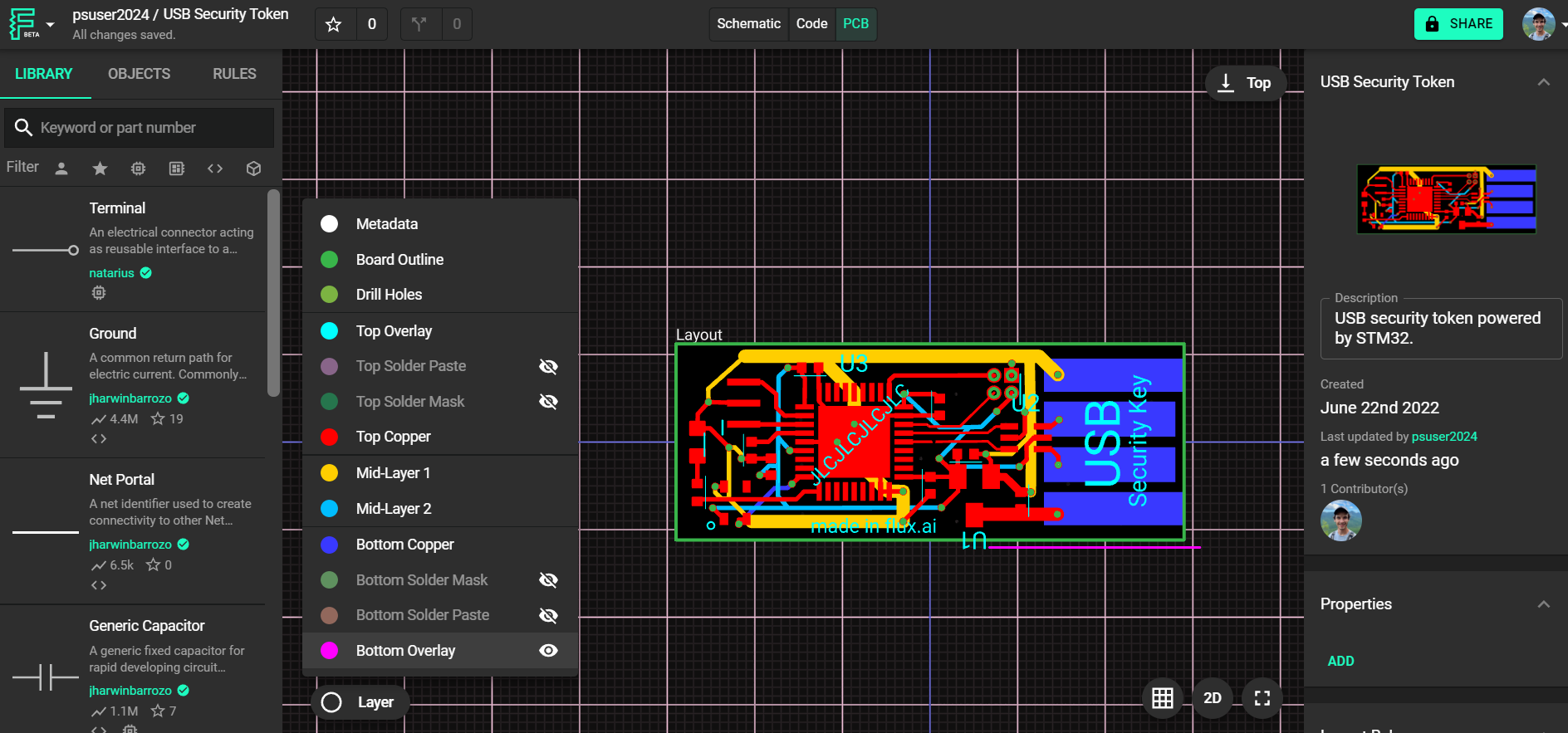
Click the Layers icon in the lower-left corner of the canvas.
A panel will open showing all layers and metadata in your PCB stackup.
Use the eye icon to toggle visibility for each layer.
For layers with copper fills, use the paint drop icon to toggle the fill rendering.
What About 3D View?
The 3D PCB view is optimized for a high-level, realistic visualization of your board. It doesn’t include layer selection controls. Here’s what you can and can’t configure:
What You Can Do in 3D View:
Rotate, pan, and zoom the board to inspect the overall geometry.
See stacked vias, components, and general board structure.
Visually confirm copper pours and silkscreen placement.
What You Can’t Do:
You cannot toggle individual layer visibility.
You cannot hide or isolate specific copper layers or metadata layers (like net or DRC overlays).
If you need to inspect specific layers or debug layer-specific issues, switch back to the 2D view using the View Mode toggle, or use Alt + 3 (⌥ + 3 on Mac) to switch between 2D and 3D camera modes in the PCB editor.
Want More Layers?
Looking to add more layers to your design? Check out Multi-Layer PCB Design.