
Flux is an AI hardware engineer. It routes your PCB, tunes pairs and lengths, and edits existing routes as part of the complete device you design.
Ask Flux to route the whole board or the nets and connections you name. You can also select traces, vias, or parts in the PCB editor and ask Flux about the selection.
Prepare the board for routing
Ask Flux to review the routing inputs before it routes the board.
Open Chat and describe your routing requirements. Routing uses the schematic nets, board size, stackup, and width and clearance rules. Ask Flux to set these up as part of your request.
For stackup and impedance setup, see Impedance control and the Stackup Editor.
Route the whole board
Ask Flux to route the whole board. You can pause board routing and resume it later.
Open Chat and send your board routing request. Send a pause or resume request in the conversation when you need it.
Route selected connections
Ask Flux to route only the nets or connections you name, or use a selection in the PCB editor.
Select traces, vias, or parts in the PCB editor. Open Chat and describe the work you want on the selection. Flux sees the selected objects.
Set power trace widths
Ask Flux to route power rails, switch nodes, and ground with widths from the current requirements or width rules. Flux can connect power and ground pads to copper planes with vias.
Open Chat and name the net and its current or trace width. For more prompts and trace-width rules, see Set power trace widths.
Choose routing layers
Tell Flux which layers to use for power, signals, and high-speed routes.
Open Chat and name the layers for each net or group. See Stackup Editor to set the board's layers and layer properties.
Route a flex or rigid-flex board
Ask Flux to route your flex or rigid-flex board with the layer and via rules of each area.
Open Chat and name the layers and areas for the routes. See Flex and Rigid-Flex Boards.
Route differential pairs
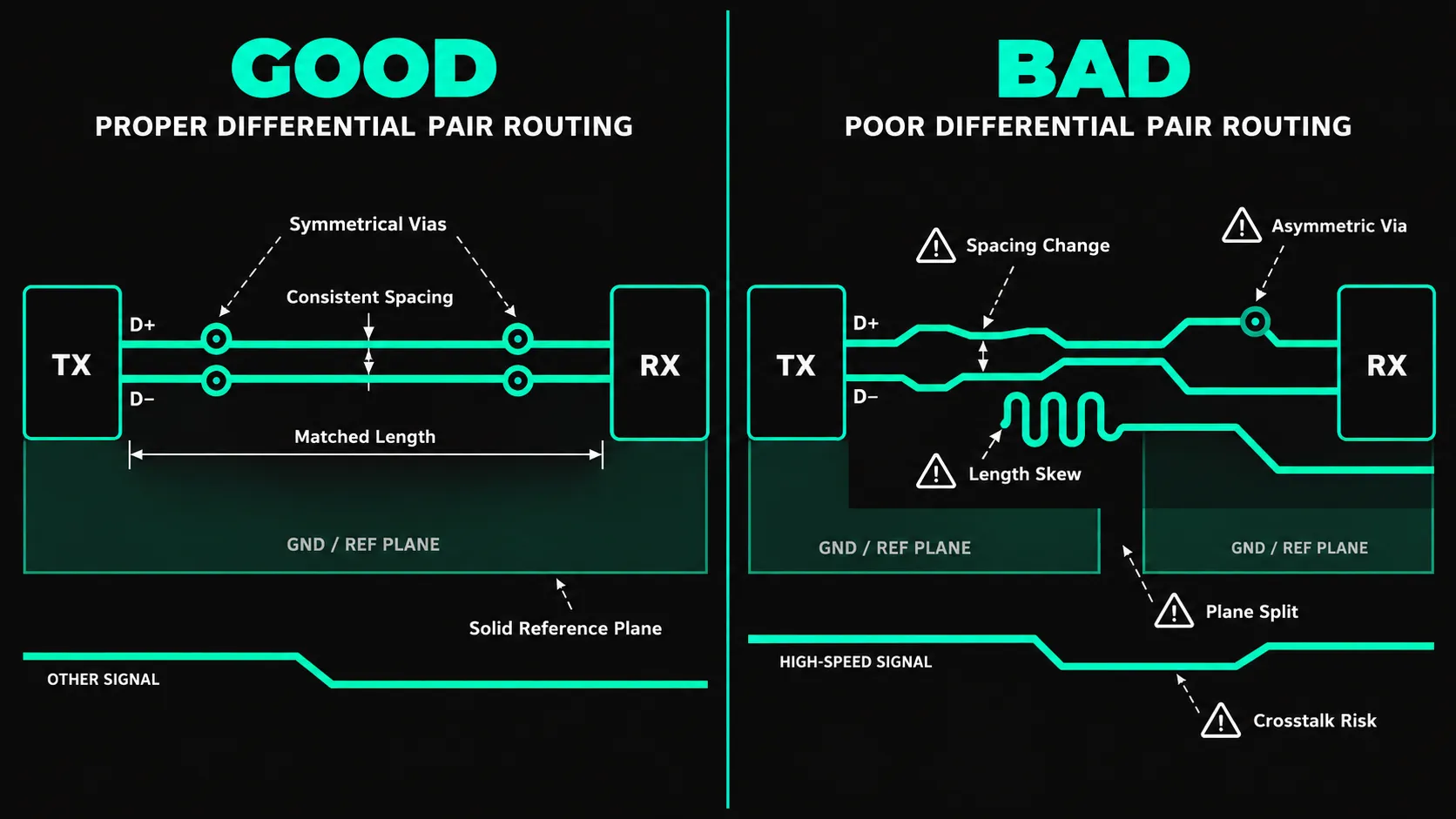
Ask Flux to route a differential pair with the pair width, gap, and skew requirements.
Set the pair properties and target impedance before routing. See Impedance control for pair setup and Positioning and routing for the editor workflow.
Route high-speed interfaces and match lengths
Ask Flux to route high-speed nets, tune their lengths, and match them within a tolerance.
Open the Chat panel and name the interface, target impedance, and length tolerance. Review the layer and impedance rules in the Stackup Editor. Flux routes the pairs and tunes their lengths to the requested tolerance. For analysis of routed signals, see Signal integrity.
You can ask Flux to route clocks and interfaces such as USB, DDR, HDMI, LVDS, and PCIe. For buses and parallel groups, specify lane order and pitch.
Tune lengths and skew
Ask Flux to tune a net to an absolute length or match its pin-to-pin length to another net. Set a tolerance in millimeters and a maximum skew for a differential pair or group. Flux reports lane lengths and skew in the result. Trombone meanders are the default. You can also ask for accordion or sawtooth meanders.
Plan DDR topology and timing budgets
Ask Flux to plan the topology of a DDR interface before it routes. Flux selects fly-by or T-branch routing for the address, command, and clock nets, and adds the termination. Flux calculates a timing budget from the trace lengths and the propagation delay of the stackup. Flux then sets the length and skew targets from that budget and routes to them.
Route RF and antenna feed lines
Ask Flux to route an RF or antenna feed line with its stackup requirements.
Open Chat and name the feed net, reference layer, and routing requirements.
Fan out dense parts
Ask Flux to fan out a BGA or route connections from fine-pitch ICs, QFNs, and dense connectors.
Flux fans out BGA pads, uses neckdowns where needed, and repairs via acid traps with short dogbone traces. For HDI routing, configure blind, buried, or microvias in the stackup. See Vias in PCB Design.
Open Chat and name the parts or select them in the PCB editor before you ask.
Break out a USB-C connector
Ask Flux to connect the USB-C pins to the board nets and route the required signals.
Open Chat and name the connector and pair requirements. For connector placement and board fit, see PCB placement.
Refine, edit, or remove routes
Ask Flux to change trace width, layer, geometry, or bend radius. You can also ask it to reroute connections or delete copper.
Select the relevant traces or vias in the PCB editor, then open Chat and describe the edit. For deletion, you can name a trace, a net, or an area. Flux skips protected copper when it deletes copper. Ask for a reroute to replace existing copper and reconnect the pads, or ask for deletion to remove copper without reconnecting.
Keep your existing copper and approve changes
Ask Flux to preserve your copper and placement when you request routing.
Flux asks before it changes your copper, your layout rules, or moves your parts. You approve each change. A routing request stays routing only unless you ask for placement work.
For each change, Flux names what it wants to change, the old and new values, and a recommended default. This includes trace width, clearance, and via rules, the Via In Pad rule, the board size, cuts into protected copper fills, and copper you drew. Flux keeps the protection state of your copper unchanged and moves only the parts you approve.
Read the proposed change in Chat and reply with the changes you approve.
Review open connections
Ask Flux to list open connections and explain what blocks them.
Flux runs airwire and design rule checks (DRC) when it finishes routing. Its report lists each open connection with its net, pin pair, what blocks it, and a proposed change. Changes can include a rule or layer change, more signal layers, a part move, or a larger board.
Read the report in Chat and answer the question to choose the next change. Open the project drawer and select Review to see the design checks.